MOSFETs - ECE @ TAMU
advertisement
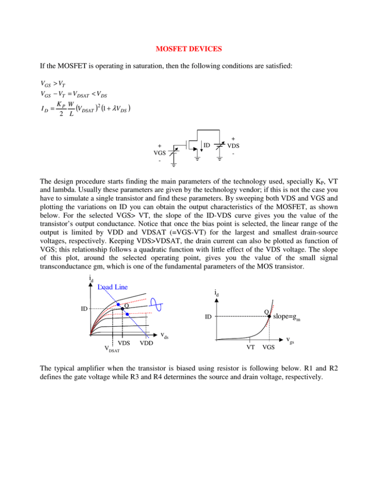
MOSFET DEVICES If the MOSFET is operating in saturation, then the following conditions are satisfied: VGS > VT VGS − VT = V DSAT < V DS ID = KP W (V DSAT )2 (1 + λV DS ) 2 L + VGS - + VDS - ID The design procedure starts finding the main parameters of the technology used, specially KP, VT and lambda. Usually these parameters are given by the technology vendor; if this is not the case you have to simulate a single transistor and find these parameters. By sweeping both VDS and VGS and plotting the variations on ID you can obtain the output characteristics of the MOSFET, as shown below. For the selected VGS> VT, the slope of the ID-VDS curve gives you the value of the transistor’s output conductance. Notice that once the bias point is selected, the linear range of the output is limited by VDD and VDSAT (=VGS-VT) for the largest and smallest drain-source voltages, respectively. Keeping VDS>VDSAT, the drain current can also be plotted as function of VGS; this relationship follows a quadratic function with little effect of the VDS voltage. The slope of this plot, around the selected operating point, gives you the value of the small signal transconductance gm, which is one of the fundamental parameters of the MOS transistor. id Load Line id Q ID Q ID VDS VDSAT VDD slope=gm vds VT VGS vgs The typical amplifier when the transistor is biased using resistor is following below. R1 and R2 defines the gate voltage while R3 and R4 determines the source and drain voltage, respectively. VDD R1 R3 vout vi R2 R4 For the definition of the operating point, similarly to the case of bipolar devices, two equations must be solved. For the output, we can write VDD = VDS + I D (R 3 + R 4) This equation can be plotted on top of the transistor’s output characteristic leading to the load line; selecting the proper VGS (defined by R1 and R2), the intersection of the transistor curve (corresponding to the selected VGS) and the load line determines the operating point Q. The transistor’s drain current must be computed by the following equation. ID = KP W 2 L (VDSAT )2 (1 + λVDS ) For hand calculations, and to solve the equations more easily, you can neglect the lambda effects; usually the error introduced is less than 5 %. Similarly, for the gate voltage and since IG=0, we obtain VG = R2 VDD R1 + R 2 and VG = VGS + ID * R 4 For the analysis and design of circuits using MOS devices you should follow the following procedure: 1. Get the value of the threshold voltage VTO (1 V in this case, but this value depends on the technology used). IF THIS VALUE IS NOT GIVEN, MAKE A VGS-ID CHARACTERIZATION, PLOT IT IN LOG SCALE AND MAKE AN EXTRAPOLATION TO FIND IT. id ID 0.1µA VT vgs 2. Find the value of KP (=uo*COX), this parameter and the gate dimensions W/L and VDSAT define the transconductance gain of the selected technology (KP ~ 10-4 A/V2 and 0.4*10-4 A/V2 for the N-MOS and P-MOS devices, respectively). 3. The lambda factor is very important for the computation of transistor’s output resistance. Find it from the ID-VDS characteristics, similarly to the case of the BJT. Schematic used for SPICE simulations Before you start the simuations, YOU MUST TO EDIT THE MODEL OF YOUR TRANSISTOR: 1) SELECT IT FROM THE SCHEMATIC 2) GO TO EDIT, AND SELECT MODEL 3) EDIT THE MODEL AS FOLLOWS (I’m using transistor MbreakND-X) .model MbreakND-X NMOS level=2 vto=1.0 tox=238e-10 nsub=33.3e15 ld=-0.05e-6 uo=515 ucrit=28.7e4 vmax=77.3e3 delta=0.0 nfs=0.45e12 rsh=25 js=.01e-3 cgdo=2.9e-10 cgso=2.9e-10 cj=3.4e-4 cjsw=2.5e-10 mj=0.430 mjsw=0.19 pb=0.96 wd=0.40e-6 xj=0.175e-6 cgbo=1.7e-10 uexp=0.251 kf=0.101e-25 neff=5.25 utra=0 af=1.33 *$ Check the operating point of your transistor (DC ANALYSIS). Analyze the result of the output file. You can find the following information: **** MOSFETS NAME M_M6 MODEL MbreakND-X ID 1.69E-03 VGS 1.67E+00 VDS 3.31E+00 VBS 0.00E+00 VTH 9.43E-01 VDSAT 4.89E-01 Lin0/Sat1 -1.00E+00 if -1.00E+00 ir -1.00E+00 TAU -1.00E+00 GM 4.28E-03 GDS 7.08E-05 GMB 1.17E-03 CBD 3.67E-14 CBS 5.90E-14 CGSOV 2.88E-14 CGDOV 2.88E-14 CGBOV 1.87E-16 CGS 1.06E-13 CGD 0.00E+00 CGB 0.00E+00 AV = − g m (RL || ro ) Compare your hand calculations with SPICE results! The hand calculations give us the following parameters: Parameter Voltage Gain Drain Current Gm KP Computed -6 (15 dB) 1.8 mA 6 mA/V 100 µA/V2 PSPICE -4 (12 dB) 1.67 mA 4.2 mA/V 74 µA/V2 Note that the voltage gain is off by a large percentage. The explanation of this difference is the value used for KP! For hand calculations we used KP=100 µA/V2, but using KP=74 µA/V2, it leads to a gm=4.4 mA/V and the voltage gain is around -4.4 V/V, which is very close to the results obtained from SPICE. After these considerations, analyze both AC and transient results! 10 0 -10 10Hz 100Hz VDB(M6:d) 1.0KHz 10KHz 100KHz Frequency AC results for the circuit 1.0MHz 10MHz 100MHz 3.6V 3.4V 3.2V 3.0V 0s 100us 200us 300us 400us 500us V(M6:d) Time Transient response of the CMOS amplifier with an input signal of 50 mVpk. AC output is close to 200 mVpk, leading to a gain of 4 (12 dB); this value is in good agreement with the result obtained form the AC analysis. DO SOME SIMULATIONS YOURSELF! Try two or 3 stage amplifiers! For gain of 100 for instance! Can you solve the non-linear equations for DC analysis? Just try to solve: I D 0 = 0 .5 K P = 0.5 K P W (VG − VS − VT )2 L W (VG − I D 0 R3 − VT )2 L 2nd order equation needs to be solved! For that reason, circuit designers prefer to use DC current sources for biasing the CMOS transistor.

