Cubic Phase HfO2 Epitaxial Thin Films Grown by MBE
advertisement
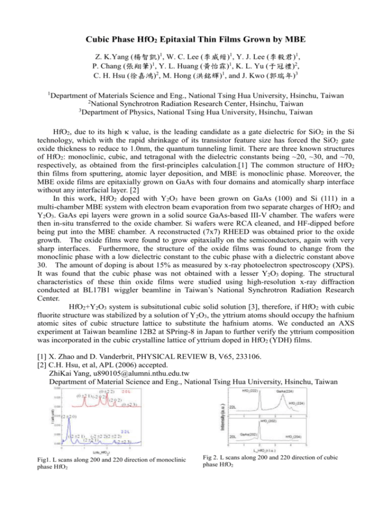
Cubic Phase HfO2 Epitaxial Thin Films Grown by MBE Z. K.Yang (楊智凱)1, W. C. Lee (李威縉)1, Y. J. Lee (李毅君)1, P. Chang (張翔筆)1, Y. L. Huang (黃怡霖)1, K. L. Yu (于冠禮)2, C. H. Hsu (徐嘉鴻)2, M. Hong (洪銘輝)1, and J. Kwo (郭瑞年)3 1 Department of Materials Science and Eng., National Tsing Hua University, Hsinchu, Taiwan 2 National Synchrotron Radiation Research Center, Hsinchu, Taiwan 3 Department of Physics, National Tsing Hua University, Hsinchu, Taiwan HfO2, due to its high value, is the leading candidate as a gate dielectric for SiO2 in the Si technology, which with the rapid shrinkage of its transistor feature size has forced the SiO2 gate oxide thickness to reduce to 1.0nm, the quantum tunneling limit. There are three known structures of HfO2: monoclinic, cubic, and tetragonal with the dielectric constants being ~20, ~30, and ~70, respectively, as obtained from the first-principles calculation.[1] The common structure of HfO2 thin films from sputtering, atomic layer deposition, and MBE is monoclinic phase. Moreover, the MBE oxide films are epitaxially grown on GaAs with four domains and atomically sharp interface without any interfacial layer. [2] In this work, HfO2 doped with Y2O3 have been grown on GaAs (100) and Si (111) in a multi-chamber MBE system with electron beam evaporation from two separate charges of HfO2 and Y2O3. GaAs epi layers were grown in a solid source GaAs-based III-V chamber. The wafers were then in-situ transferred to the oxide chamber. Si wafers were RCA cleaned, and HF-dipped before being put into the MBE chamber. A reconstructed (7x7) RHEED was obtained prior to the oxide growth. The oxide films were found to grow epitaxially on the semiconductors, again with very sharp interfaces. Furthermore, the structure of the oxide films was found to change from the monoclinic phase with a low dielectric constant to the cubic phase with a dielectric constant above 30. The amount of doping is about 15% as measured by x-ray photoelectron spectroscopy (XPS). It was found that the cubic phase was not obtained with a lesser Y2O3 doping. The structural characteristics of these thin oxide films were studied using high-resolution x-ray diffraction conducted at BL17B1 wiggler beamline in Taiwan’s National Synchrotron Radiation Research Center. HfO2+Y2O3 system is subsitutional cubic solid solution [3], therefore, if HfO2 with cubic fluorite structure was stabilized by a solution of Y2O3, the yttrium atoms should occupy the hafnium atomic sites of cubic structure lattice to substitute the hafnium atoms. We conducted an AXS experiment at Taiwan beamline 12B2 at SPring-8 in Japan to further verify the yttrium composition was incorporated in the cubic crystalline lattice of yttrium doped in HfO2 (YDH) films. [1] X. Zhao and D. Vanderbrit, PHYSICAL REVIEW B, V65, 233106. [2] C.H. Hsu, et al, APL (2006) accepted. ZhiKai Yang, u890105@alumni.nthu.edu.tw Department of Material Science and Eng., National Tsing Hua University, Hsinchu, Taiwan Fig1. L scans along 200 and 220 direction of monoclinic phase HfO2 Fig 2. L scans along 200 and 220 direction of cubic phase HfO2
