II. the multiple-peak MOS
advertisement
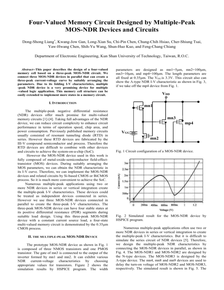
Four-Valued Memory Circuit Designed by Multiple-Peak MOS-NDR Devices and Circuits Dong-Shong Liang*, Kwang-Jow Gan, Long-Xian Su, Chi-Pin Chen, Chung-Chih Hsiao, Cher-Shiung Tsai, Yaw-Hwang Chen, Shih-Yu Wang, Shun-Huo Kuo, and Feng-Chang Chiang Department of Electronic Engineering, Kun Shan University of Technology, Taiwan, R.O.C. Abstract--This paper describes the design of a four-valued memory cell based on a three-peak MOS-NDR circuit. We connect three MOS-NDR devices in parallel that can create a three-peak current-voltage curve by suitably arranging the parameters. Due to its folding I-V characteristics, multiple -peak NDR device is a very promising device for multiple -valued logic application. This memory cell structure can be easily extended to implement more states in a memory circuit. parameters are designed as mn1=5μm, mn2=100μm, mn3=10μm, and mp4=100μm. The length parameters are all fixed at 0.35μm. The VGG is 3.3V. This circuit also can show the Λ-type NDR I-V characteristic as shown in Fig. 3, if we take off the mp4 device from Fig. 1. VDD I. INTRODUCTION The multiple-peak negative differential resistance (NDR) devices offer much promise for multi-valued memory circuits [1]-[4]. Taking full advantages of the NDR device, we can reduce circuit complexity to enhance circuit performance in terms of operation speed, chip area, and power consumption. Previously published memory circuits usually consisted of resonant tunneling diode (RTD) in series. However these RTD devices are fabricated by the III-V compound semiconductor and process. Therefore the RTD devices are difficult to combine with other devices and circuits to achieve the system-on-a-chip (SoC). However the MOS-NDR device used in this work is fully composed of metal-oxide-semiconductor field-effecttransistor (MOS) devices. During suitably arranging the MOS parameters, we can obtain the NDR characteristic in its I-V curve. Therefore, we can implement the MOS-NDR devices and related circuits by Si-based CMOS or BiCMOS process. So it is much more convenient to achieve the SoC. Numerous multiple-peak applications using two or more NDR devices in series or vertical integration create the multiple-peak I-V characteristics. These devices could be treated as independent devices connected in series. However we use three MOS-NDR devices connected in parallel to create the three-peak I-V characteristics. The three-peak MOS-NDR device can have four stable states at its positive differential resistance (PDR) segments during suitable load design. Using this three-peak MOS-NDR device with a constant current source load, a four-state multi-valued memory circuit is demonstrated by the 0.35μm CMOS process. II. THE MULTIPLE-PEAK MOS-NDR DEVICE The prototype MOS-NDR device as shown in Fig. 1 is composed of three NMOS transistors and one PMOS transistor. The gate of mn3 is connected to the output of the inverter formed by mn1 and mn2. It can exhibit various NDR current-voltage characteristics by choosing appropriate values for transistors. Figure 2 shows the simulation results by HSPICE program. The width mn1 mn3 mp4 VGG mn2 Fig. 1 Circuit configuration of a MOS-NDR device. Fig. 2 Simulated result for the MOS-NDR device by HSPICE program. Numerous multiple-peak applications often use two or more NDR devices in series or vertical integration to create the multiple-peak I-V characteristics. But it is difficult to simulate the series circuit of NDR devices [5]. Therefore, we design the multiple-peak NDR characteristics by connecting the MOS-NDR devices in parallel, as shown in Fig. 4. The MOS-NDR1 and MOS-NDR2 are designed by the N-type devices. The MOS-NDR3 is designed by the Λ-type device. The mn4, mn8 and mn9 devices are used to delay the turn-on voltage of MOS-NDR2 and MOS-NDR3, respectively. The simulated result is shown in Fig. 5. The Vgg voltages are all fixed at 3.3V. R V1 V2 current source V3 V4 Fig. 3 Simulated result for the Λ-type I-V characteristic. Fig. 6 The I-V characteristics for multiple-valued memory circuit using either a resistor load or a constant current source. If a constant current source is used as the load device, the current could be adjusted through appropriate device parameters to a value approximately halfway between the peak and valley current of the multiple-peak NDR device. By comparing to the resistor load configuration, the memory circuit using the constant current source as the load device has two advantages, the better noise margins for the four stable states and the low power dissipation [6]. Fig. 4 Circuit configuration of the multiple-peak MOSNDR device. Fig. 5 Simulated result for the multiple-peak MOS-NDR device. III. MULTIPLE –VALUED MEMORY CIRCUIT DESIGN Due to the folding I-V characteristics, multiple-peak NDR device is a very promising device for multi-valued logic application. The obvious method to bias the multiple-peak NDR device into the multiple stable states is to use a resistor or a constant current source as a load, as shown in Fig. 6, respectively. For the three-peak MOS-NDR device, there are at most four stable states from V1 to V4. When the series resistor exceeds the magnitude of the NDR of the multiple-peak device, the series resistor can be considered as a load resistance which intersects the PDR regions of the multiple-peak device at multiple stable states. When one locates the stable points, one always locates the points of intersection on the PDR region because all the intersection points on the NDR region are always unstable. Fig. 7 The four-valued MOS-NDR memory circuit. Figure 7 shows the four-state MOS-NDR memory circuit. The voltage to be stored is provided at the cell input and loaded by momentarily enabling the write clock. The input voltage then controls the voltage at the multiple-peak MOS-NDR node. When the write clock is disabled, the voltage across the MOS-NDR device adjusts to the nearest stable operating point, thereby storing the input value at one of the four discrete levels. A saw-tooth wave is applied to the input of the memory circuit with amplitude of 3.5V. A square wave is then applied to the write gate input which alternately turns the MOS on and off. The output of this memory circuit gives the four stable memory values, as shown in Fig. 8. We can understand the attractive feature for this memory circuit for the constant-current-source load is that the noise margin would remain the same with a further increase in the number of current peaks of the multiple-peak MOS-NDR device. The design of this memory circuit is demonstrated by the standard 0.35μm CMOS process. We design the constant current source by the MOS devices. effort and assistance in arranging the fabrication of this chip. This work was supported by the National Science Council of Republic of China under the contract no. NSC93-2218E-168-002. REFERENCES Fig. 8 Simulated results for the MOS-NDR memory circuit. V. CONCLUSIONS In this work, we have demonstrated the three-peak MOS-NDR circuit with three MOS-NDR devices connected in parallel. The series combination of this device with a constant-current-source load is used to demonstrate the operation of a four stable state memory cell. Because all of the devices used in this circuit are fully composed of MOS devices, we can fabricate this memory circuit by the standard Si-based CMOS or BiCMOS process. Furthermore, this MOS-NDR device and circuit will be easy to integrate with other device and circuit to achieve the goal of SoC. ACKNOWLEDGMENTS The authors would like to thank the Chip Implementation Center (CIC) of Taiwan for their great [1] S. Sen, F. Capasso, A. Y. Cho, and D. Sivco, “Resonant tunneling device with multiple negative differential resistance: digital and signal processing applications with reduced circuit complexity,”IEEE Trans. Electron Devices, vol. 34, pp. 2185-2191, 1987. [2] J. P. A. van der Wagt, H. Tang, T. P. E. Broekaert, A. C. Seabaugh, and Y. C. Kao, ”Multibit resonant tunneling diode SRAM cell based on slew-rate addressing,” IEEE Trans. Electron Devices, vol. 46, pp. 55-62, 1999. [3] S. J. Wei and H. C. Lin, “Multivalued SRAM cell using resonant tunneling diodes,” IEEE J. Solid-St. Circuits, vol. 27, pp. 212-216, 1992. [4] A. C. Seabaugh, Y. C. Kao, and H. T. Yuan, ”Nine-state resonant tunneling diode memory,” IEEE Electron Device Lett., vol. 13, pp. 479-481, 1992. [5] K. J. Gan“Hysteresis phenomena for the series circuit of two identical negative differential resistance devices,”Japanese Journal of Applied Physics, Vol. 40, No. 4A, pp. 2159-2164, 2001. [6] Z. X. Yan and M. J. Deen, ”A new resonant-tunnel diode-based multivalued memory circuit using a MESFET depletion load,” IEEE J. Solid-State Circuits, vol. 27, pp. 1198-1202, 1992.

