Solar Wafer Size Standards: M1 & M2 Specifications
advertisement
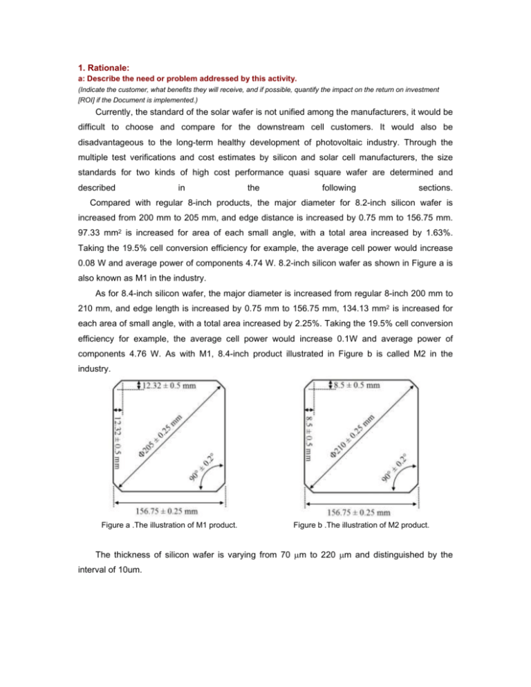
1. Rationale: a: Describe the need or problem addressed by this activity. (Indicate the customer, what benefits they will receive, and if possible, quantify the impact on the return on investment [ROI] if the Document is implemented.) Currently, the standard of the solar wafer is not unified among the manufacturers, it would be difficult to choose and compare for the downstream cell customers. It would also be disadvantageous to the long-term healthy development of photovoltaic industry. Through the multiple test verifications and cost estimates by silicon and solar cell manufacturers, the size standards for two kinds of high cost performance quasi square wafer are determined and described in the following sections. Compared with regular 8-inch products, the major diameter for 8.2-inch silicon wafer is increased from 200 mm to 205 mm, and edge distance is increased by 0.75 mm to 156.75 mm. 97.33 mm2 is increased for area of each small angle, with a total area increased by 1.63%. Taking the 19.5% cell conversion efficiency for example, the average cell power would increase 0.08 W and average power of components 4.74 W. 8.2-inch silicon wafer as shown in Figure a is also known as M1 in the industry. As for 8.4-inch silicon wafer, the major diameter is increased from regular 8-inch 200 mm to 210 mm, and edge length is increased by 0.75 mm to 156.75 mm, 134.13 mm2 is increased for each area of small angle, with a total area increased by 2.25%. Taking the 19.5% cell conversion efficiency for example, the average cell power would increase 0.1W and average power of components 4.76 W. As with M1, 8.4-inch product illustrated in Figure b is called M2 in the industry. Figure a .The illustration of M1 product. Figure b .The illustration of M2 product. The thickness of silicon wafer is varying from 70 m to 220 m and distinguished by the interval of 10um.
