srep03667
advertisement
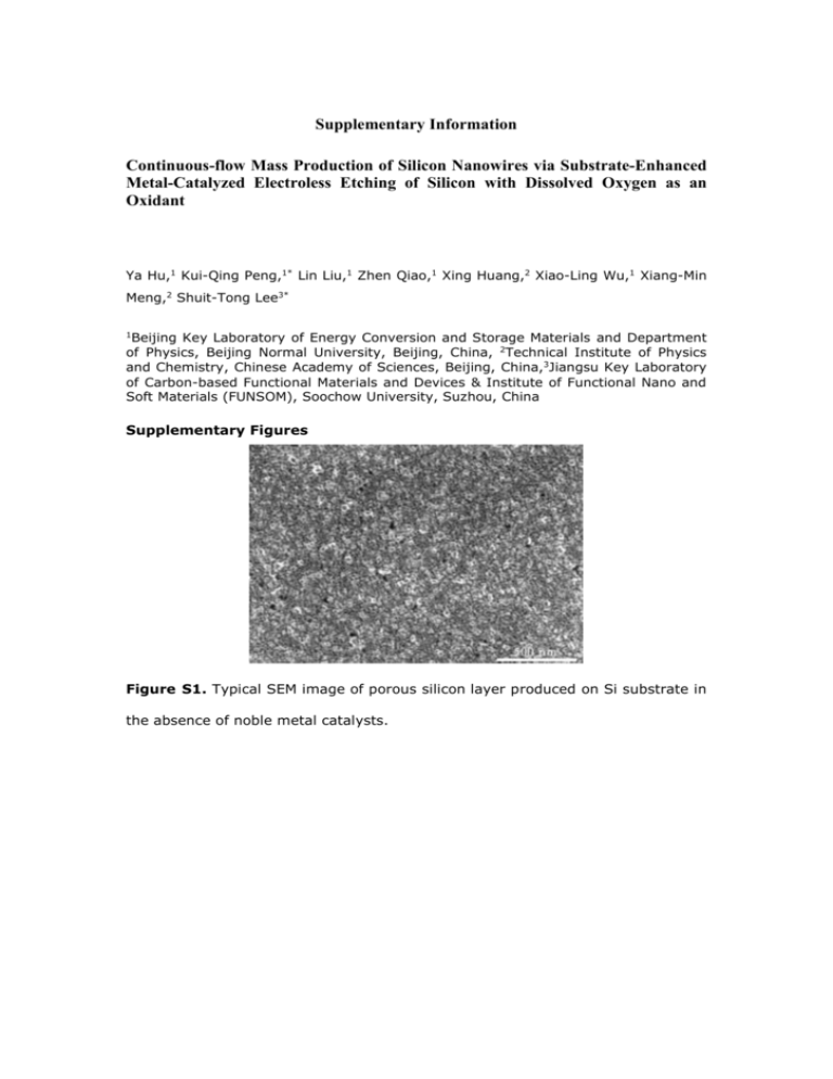
Supplementary Information Continuous-flow Mass Production of Silicon Nanowires via Substrate-Enhanced Metal-Catalyzed Electroless Etching of Silicon with Dissolved Oxygen as an Oxidant Ya Hu,1 Kui-Qing Peng,1* Lin Liu,1 Zhen Qiao,1 Xing Huang,2 Xiao-Ling Wu,1 Xiang-Min Meng,2 Shuit-Tong Lee3* Beijing Key Laboratory of Energy Conversion and Storage Materials and Department of Physics, Beijing Normal University, Beijing, China, 2Technical Institute of Physics and Chemistry, Chinese Academy of Sciences, Beijing, China,3Jiangsu Key Laboratory of Carbon-based Functional Materials and Devices & Institute of Functional Nano and Soft Materials (FUNSOM), Soochow University, Suzhou, China 1 Supplementary Figures Figure S1. Typical SEM image of porous silicon layer produced on Si substrate in the absence of noble metal catalysts. Figure S2. High-resolution TEM image of a mesoporous Si nanowire produced from a p-type 0.001-0.008 Ω·cm Si(100) wafer. Figure S3. SEM image of ordered silicon nanohole array produced on a p-type 110 Ω·cm Si(100) wafer. Figure S4. SEM image of AgNPs-induced shallow pits on the surface of a p-type 1-10 Ω · cm Si(100) wafer after 3-hours immersion in aqueous HF solution. Graphite or noble metal board was not used.
