Q1: For the circuit shown below:
advertisement
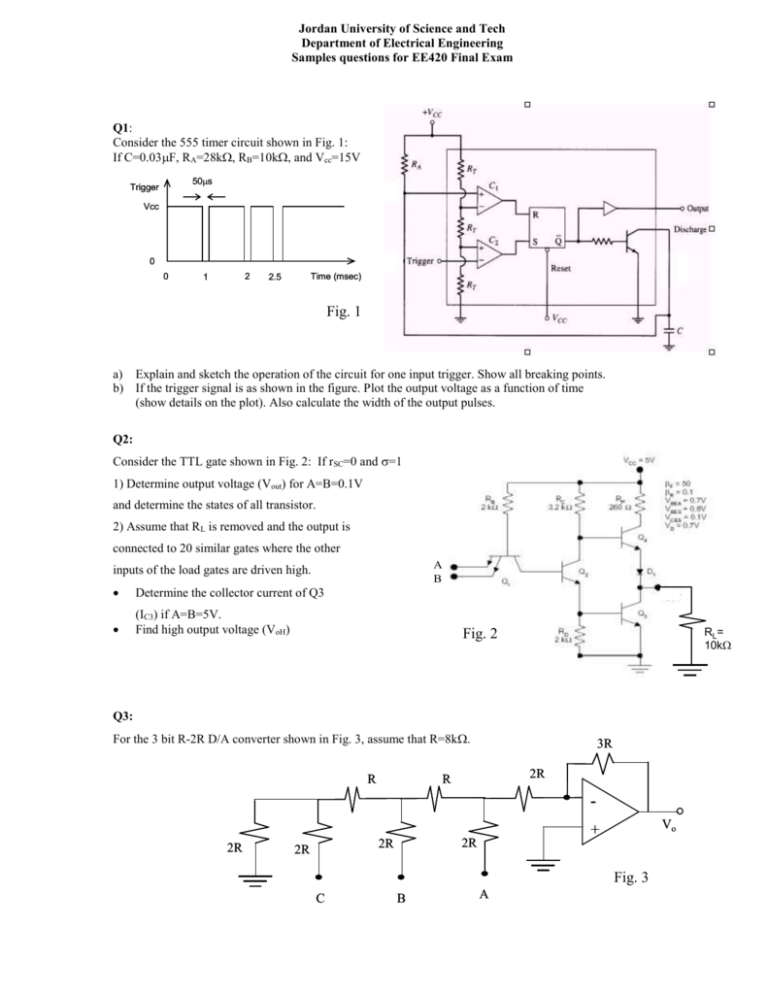
Jordan University of Science and Tech Department of Electrical Engineering Samples questions for EE420 Final Exam Q1: Consider the 555 timer circuit shown in Fig. 1: If C=0.03F, RA=28k, RB=10k, and Vcc=15V 50s Trigger Vcc 0 0 2 1 Time (msec) 2.5 Fig. 1 a) Explain and sketch the operation of the circuit for one input trigger. Show all breaking points. b) If the trigger signal is as shown in the figure. Plot the output voltage as a function of time (show details on the plot). Also calculate the width of the output pulses. Q2: Consider the TTL gate shown in Fig. 2: If rSC=0 and =1. 1) Determine output voltage (Vout) for A=B=0.1V and determine the states of all transistor. 2) Assume that RL is removed and the output is connected to 20 similar gates where the other A B inputs of the load gates are driven high. Determine the collector current of Q3 (IC3) if A=B=5V. Find high output voltage (VoH) RL = 10k Fig. 2 Q3: For the 3 bit R-2R D/A converter shown in Fig. 3, assume that R=8k. R 3R 2R R Vo + 2R 2R 2R 2R Fig. 3 C B A a) What is the advantage of this circuit over weighted D/A converters b) If A=0V, B=5V and C=5V find Vo 5V Q4: For the CMOS circuit shown in Fig. 4: If Q2 as K2=200A/V2 and VT2=-0.3V while Q1 has K1=150A/V2 and VT1=0.6V Q2 a) Draw the transfer characteristics showing status of Q1 and Q2. b) Determine the range of Vin and Vo for each mode of operation (cutoff, saturation, and ohmic (linear)) of Q 1. c) Find the maximum current passing through the circuit and find the corresponding Vin. Vin Q1 Vo Fig. 4 10V Q5: Consider the TTL to CMOS interface circuit Shown in Fig. 5: If the TTL gates have VoL=0.5V and VOH=3V 1k 5V 10V R2 R1 For CMOS, the input voltage for logic zero is 0.2V and the input voltage for logic one is 10V Q2 Q1 Find R1 and R2 such that the TTL gate can be interfaced with the CMOS gate. Assume that =60, VCES=0.2V, VBEA=0.7V, VBES=0.8V; TTL CMOS Fig. 5 Q6: Consider the Schmitt trigger circuit shown in Fig 6: If Vcc=12V 12k 6k VCC Vin a) Plot Vo versus Vin and find the hysteresis b) Plot Vo(t) show all details on the plot + 6V Vcc - Vin 2 1 3 Vo -VCC Time (msec) -Vcc Fig. 6 If the circuit is modified as shown in Fig. 7 c) Calculate the frequency of the output d) Duty cycle of the output e) Plot the voltage across the capacitor showing the maximum and minimum voltages. 12k 6k 6V 12V + 1F -12V 1k Fig. 7 Vo Q7: Consider the TTL gate shown in Fig. 8: If Q1 has =70 and I=R=0.1. If the output of the gate is connected to 30 similar gates and VA=VB=VCC. Find 1k a) collector current for Q0 b) the base current for Q0 c) The minimum value of for Qo. Assume that VB for all loaded gates are connected to logic zero (VB=0.1V for load transistors) Q8: VCC VCC Consider the 555 timer circuit shown in Fig. 9: a) Explain the operation of the circuit, and plot the voltage across the capacitor and the output voltage for one cycle b) Design an Astable multivibrator which produce 5kHz output with 75% duty cycle use C=0.1F. c) Modify the circuit such that it works As a Monostable where the circuit produces 1ms output pulse using C=0.1F. See Next page R RA VCC Output RB R VCC C R Fig. 9 R Q S Q’ Tx
