EE201 Electrical Engineering Laboratory
advertisement
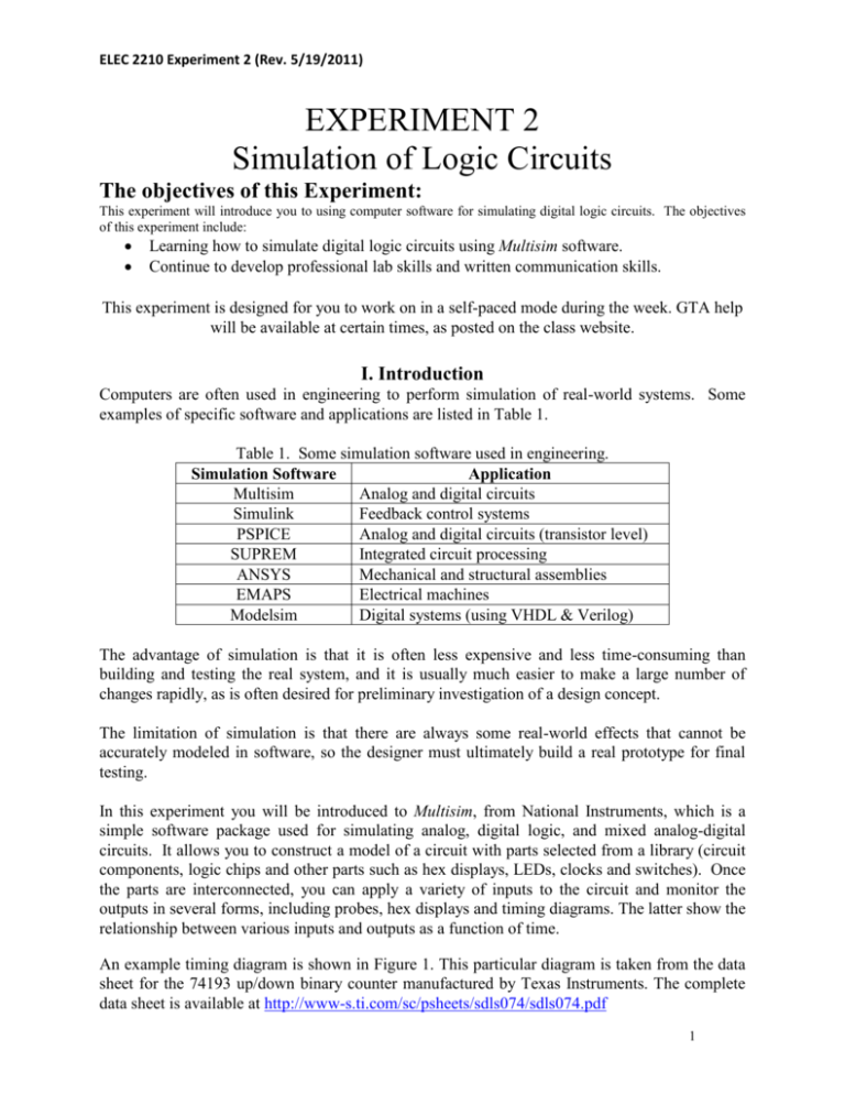
ELEC 2210 Experiment 2 (Rev. 5/19/2011) EXPERIMENT 2 Simulation of Logic Circuits The objectives of this Experiment: This experiment will introduce you to using computer software for simulating digital logic circuits. The objectives of this experiment include: Learning how to simulate digital logic circuits using Multisim software. Continue to develop professional lab skills and written communication skills. This experiment is designed for you to work on in a self-paced mode during the week. GTA help will be available at certain times, as posted on the class website. I. Introduction Computers are often used in engineering to perform simulation of real-world systems. Some examples of specific software and applications are listed in Table 1. Table 1. Some simulation software used in engineering. Simulation Software Application Multisim Analog and digital circuits Simulink Feedback control systems PSPICE Analog and digital circuits (transistor level) SUPREM Integrated circuit processing ANSYS Mechanical and structural assemblies EMAPS Electrical machines Modelsim Digital systems (using VHDL & Verilog) The advantage of simulation is that it is often less expensive and less time-consuming than building and testing the real system, and it is usually much easier to make a large number of changes rapidly, as is often desired for preliminary investigation of a design concept. The limitation of simulation is that there are always some real-world effects that cannot be accurately modeled in software, so the designer must ultimately build a real prototype for final testing. In this experiment you will be introduced to Multisim, from National Instruments, which is a simple software package used for simulating analog, digital logic, and mixed analog-digital circuits. It allows you to construct a model of a circuit with parts selected from a library (circuit components, logic chips and other parts such as hex displays, LEDs, clocks and switches). Once the parts are interconnected, you can apply a variety of inputs to the circuit and monitor the outputs in several forms, including probes, hex displays and timing diagrams. The latter show the relationship between various inputs and outputs as a function of time. An example timing diagram is shown in Figure 1. This particular diagram is taken from the data sheet for the 74193 up/down binary counter manufactured by Texas Instruments. The complete data sheet is available at http://www-s.ti.com/sc/psheets/sdls074/sdls074.pdf 1 ELEC 2210 Experiment 2 (Rev. 5/19/2011) The manufacturer uses the timing diagram to graphically illustrate the effect of the various inputs on the various outputs. Careful analysis of this diagram together with the verbal description and logic tables provided in the data sheet give a complete picture of the operation of this device. Prelab Answer the following questions before attempting the experiment. It will help to download or view pages 1 and 6 of the data sheet at the given URL. Show and/or explain your work including intermediate steps. 1. For the counter to operate, what must be the logic level on the CLEAR CLR line (high or low)? 2. What are the binary and decimal values of the counter output QDQCQBQA immediately after the LOAD pulse is applied? 3. What is the output (binary and decimal) at the end of the COUNT UP interval? 4. What are the functions of the BORROW OUT BO and CARRY OUT CO signals? (see the "Description" section on the first page of the complete data sheet.) 2 ELEC 2210 Experiment 2 (Rev. 5/19/2011) Figure 1. Example timing diagram for a binary counter. 3 ELEC 2210 Experiment 2 (Rev. 5/19/2011) Lab Exercise This experiment will be performed on a computer using Multisim software. The PC lab in Broun 308 is available for your use except when reserved for other classes. Multisim is installed on each of the 12 machines in this lab. The Multisim tutorial is designed to be self-explanatory, and regardless of the availability of your instructor, you should complete this experiment on your own time in Broun 308. Report computer and network problems in 308 to the ECE IT office*. (1) Complete the Multisim "10-minute Tutorial", contained in file “Multisim_Tutorial.pdf”. Work through the tutorial to learn how to use Multisim to simulate a simple digital logic circuit. (2) Draw and simulate the 4-bit binary counter circuit shown in Figure 2, which is based on the 74163 binary counter. Use source type DIGITAL_CLOCK for the clock input and INTERACTIVE_DIGITAL_CONSTANT for all other inputs, so that you can change the inputs interactively. Connect the outputs to a logic analyzer, to capture and display a timing diagram, and a DCD_HEX_GREEN indicator to display the count value. Your counter must perform as follows: (1) When the CLR input is 0, the output should reset to 0. (2) When the CLR input is set back to 1, the output should count up. (It is recommended that you set the simulation speed to somewhere around "walk" so you can actually see the count changing. Also, the timing diagram shown in Figure 3 should be generated. When your circuit is working properly, use the text tool to put your name and the date on the diagram. Then save your circuit on your H: drive and/or your personal USB drive. (3) Print your circuit and the timing diagram to include in your lab report. You may need to use screen capture to get the hardcopy. (4) Email your circuit (.ms11) to your GTA as an attachment. The subject line in your email should read "2210 Expt 2 Circuit from userID." This counts as part of your lab report submission. Your GTA’s email address is on the lab web page. * Mr. John Newton in Broun 321, Email: jbn0002@auburn.edu 4 ELEC 2210 Experiment 2 (Rev. 5/19/2011) ENP U7 1 Key = Space ENT DCD_HEX_GREEN 1 Key = Space LOAD U1 1 Key = Space CLR 1 Key = Space CLK 1kHz 3 4 5 6 A B C D 7 10 ENP ENT 2 1 ~LOAD ~CLR 9 CLK XLA1 QA QB QC QD 14 13 12 11 RCO 15 1 74LS163D F C Q T Figure 2. Test Circuit Figure 3. Test Circuit Output (Logic Analyzer Display) 5
