T E C H N I C A L
Optima 8300 ICP-OES
Optical System
and SCD Detector
N O T E
ICP-Optical Emission
Spectroscopy
The optimized optical system of the Optima™ 8300 ICP-OES
centers on a unique high-performance solid-state detector – the
Segmented-array Charge-coupled Device (SCD) detector. A
new echelle-based polychromator was designed in order to
fully utilize the capabilities of the SCD. Using a PerkinElmer®
echelle grating optimized for UV performance and a unique
Schmidt cross-disperser grating, the Optima 8300 optical
system has exceptional optical throughput and excellent
resolution, providing you with superior detection limits and
line selection.
Why an SCD? Flexibility, simultaneity and low noise
Figure 1. The Optima 8300 SCD mounted on a Peltier cooler.
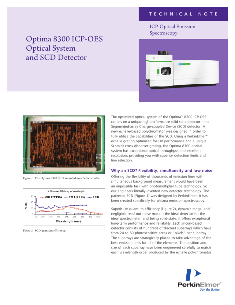
Figure 2. SCD quantum efficiency.
Offering the flexibility of thousands of emission lines with
simultaneous background measurement would have been
an impossible task with photomultiplier tube technology. So
our engineers literally invented new detector technology. The
patented SCD (Figure 1) was designed by PerkinElmer. It has
been created specifically for plasma emission spectroscopy.
Superb UV quantum efficiency (Figure 2), dynamic range, and
negligible read-out noise make it the ideal detector for the
ideal spectrometer, and being solid-state, it offers exceptional
long-term performance and reliability. Each silicon-based
detector consists of hundreds of discreet subarrays which have
from 20 to 80 photosensitive areas or “pixels” per subarray.
The subarrays are strategically placed to take advantage of the
best emission lines for all of the elements. The position and
size of each subarray have been engineered carefully to match
each wavelength order produced by the echelle polychromator.
On the detector next to each subarray (Figure 3) are the
output electronics for that subarray. Since the electronics
are immediately adjacent to the subarray, the readout noise
is extremely low, much lower than any other charge transfer device. There is no need for time-consuming multiple
readouts to reduce detector noise. Also, each subarray can
be individually addressed through the interface logic next to
it. This means that you can read any subarray without the
necessity of reading out an entire detector, thus saving you
time.
The SCD detector, unlike many Charge-Coupled Devices
(CCDs), has been designed to prevent charge “blooming.”
“Blooming” occurs when a pixel fills up with electrons and
the excess electrons spill into an adjacent pixel, much like
an overfilled bucket. Should a pixel on the SCD exceed its
capacity during an integration, the excess electrons flow
into the output register where they are electronically swept
away. For secondary protection, there is also a guard band
surrounding each subarray. This anti-blooming design helps
to ensure the integrity of your results.
Figure 3. Drawing of a single subarray from the SCD.
The subarrays see different portions of the wavelength spectrum at the same time, allowing simultaneous measurement
of thousands of emission and background wavelengths. The
peak emission and the spectral background are measured
simultaneously (with user-selectable background parameters),
reducing data-acquisition time and increasing your sample
throughput. Analytical precision and detection limits are also
improved, since simultaneous measurement of analyte and
background can compensate for signal variations attributable
to the sampling system.
The Optima 8300 ICP-OES optical system
Energy from the plasma enters the spectrometer and is
focused on the entrance slit by the torroidal mirrors (Figure 4).
The first mirror is computer-controlled and can be automatically positioned to optimize both the plasma viewing
2
height and lateral position. The second torroidal mirror
directs the plasma energy to the entrance slit. The parabolic
mirror, after the slit, collimates the energy onto the echelle
grating, which separates the light into high dispersion,
overlapping orders.
The next optical component, the Schmidt cross-disperser,
serves three purposes. First, with dual-detector configurations, a hole in the center of the optic is used to split the
light into separate UV and visible channels. Light passing
through the hole is dispersed by the prism and is focused
onto the surface of the visible wavelength detector. The
energy reflected off the surface of the cross-disperser is sent
through the UV channel. The use of separate UV and visible channels effectively doubles the detector area. It also
ensures that there are no compromises in spectral range,
resolution or energy throughput and that analyses at all
wavelengths can be performed simultaneously.
Figure 4. Optima 8300 optical diagram.
The second purpose of the Schmidt cross-disperser is to
serve as a grating that separates the light by order. The
dispersed light is sent to the camera sphere and then onto
the UV wavelength detector via the fold flat mirror, the size
and shape of which are matched to the hole in the crossdisperser so that no energy is lost.
The third use of the Schmidt cross-disperser is to optically
correct for spherical aberrations, distortions of the optical
image. By correcting for these aberrations, the Optima
spectrometer produces clean, sharp images at the detector
for highest resolution (Figure 5). To provide long-term stability,
the entire Optima 8300 optical system is enclosed in a thermostatted housing. This isolates the optical system from the
ambient environment and ensures exceptional wavelength
stability. Better stability means better productivity, because
less time is required for recalibration.
Better answers faster
Even if you don’t need to reach the trace detection limits
that the Optima 8300 ICP-OES can provide, that power
translates into improved precision, accuracy and speed, supplying clearly better analytical results, faster. Plus, you can be
assured that if your requirements change, you have
a system that has the ability to grow with you.
Figure 5. The superb resolution of the Optima 8300 ICP-OES is shown by the
separation of the boron doublet at 182.5 nm.
PerkinElmer, Inc.
940 Winter Street
Waltham, MA 02451 USA
P: (800) 762-4000 or
(+1) 203-925-4602
www.perkinelmer.com
For a complete listing of our global offices, visit www.perkinelmer.com/ContactUs
Copyright ©2002-2011, PerkinElmer, Inc. All rights reserved. PerkinElmer® is a registered trademark of PerkinElmer, Inc. All other trademarks are the property of their respective owners.
006270C_01
