64-Position Up/Down
Control Digital Potentiometer
AD5227
FEATURES
FUNCTIONAL BLOCK DIAGRAM
64-position digital potentiometer
10 kΩ, 50 kΩ, 100 kΩ end-to-end terminal resistance
Simple up/down digital or manual configurable control
Midscale preset
Low potentiometer mode tempco = 10 ppm/°C
Low rheostat mode tempco = 35 ppm/°C
Ultralow power, IDD = 0.4 µA typ and 3 µA max
Fast adjustment time, ts = 1 µs
Chip select enable multiple device operation
Low operating voltage, 2.7 V to 5.5 V
Automotive temperature range, −40°C to +105°C
Compact thin SOT-23-8 (2.9 mm × 3 mm) Pb-free package
VDD
AD5227
A
CS
6-BIT UP/DOWN
CONTROL
LOGIC
U/D
CLK
W
B
POR
MIDSCALE
WIPER
REGISTER
04419-0-001
GND
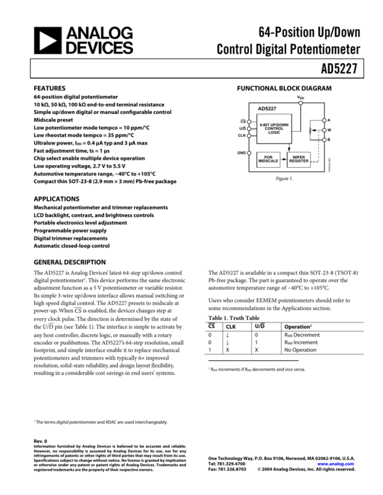
Figure 1.
APPLICATIONS
Mechanical potentiometer and trimmer replacements
LCD backlight, contrast, and brightness controls
Portable electronics level adjustment
Programmable power supply
Digital trimmer replacements
Automatic closed-loop control
GENERAL DESCRIPTION
The AD5227 is Analog Devices’ latest 64-step up/down control
digital potentiometer1. This device performs the same electronic
adjustment function as a 5 V potentiometer or variable resistor.
Its simple 3-wire up/down interface allows manual switching or
high speed digital control. The AD5227 presets to midscale at
power-up. When CS is enabled, the devices changes step at
every clock pulse. The direction is determined by the state of
the U/D pin (see Table 1). The interface is simple to activate by
any host controller, discrete logic, or manually with a rotary
encoder or pushbuttons. The AD5227’s 64-step resolution, small
footprint, and simple interface enable it to replace mechanical
potentiometers and trimmers with typically 6× improved
resolution, solid-state reliability, and design layout flexibility,
resulting in a considerable cost savings in end users’ systems.
1
The AD5227 is available in a compact thin SOT-23-8 (TSOT-8)
Pb-free package. The part is guaranteed to operate over the
automotive temperature range of −40°C to +105°C.
Users who consider EEMEM potentiometers should refer to
some recommendations in the Applications section.
Table 1. Truth Table
CS
0
0
1
1
CLK
↓
↓
X
U/D
0
1
X
Operation1
RWB Decrement
RWB Increment
No Operation
RWA increments if RWB decrements and vice versa.
The terms digital potentiometer and RDAC are used interchangeably.
Rev. 0
Information furnished by Analog Devices is believed to be accurate and reliable.
However, no responsibility is assumed by Analog Devices for its use, nor for any
infringements of patents or other rights of third parties that may result from its use.
Specifications subject to change without notice. No license is granted by implication
or otherwise under any patent or patent rights of Analog Devices. Trademarks and
registered trademarks are the property of their respective owners.
One Technology Way, P.O. Box 9106, Norwood, MA 02062-9106, U.S.A.
Tel: 781.329.4700
www.analog.com
Fax: 781.326.8703
© 2004 Analog Devices, Inc. All rights reserved.
AD5227
TABLE OF CONTENTS
Electrical Characteristics ................................................................. 3
Layout and Power Supply Biasing ............................................ 11
Interface Timing Diagrams ......................................................... 4
Applications..................................................................................... 12
Absolute Maximum Ratings............................................................ 5
Manual Control with Toggle and Pushbutton Switches........ 12
ESD Caution.................................................................................. 5
Manual Control with Rotary Encoder..................................... 12
Pin Configuration and Function Descriptions............................. 6
Adjustable LED Driver .............................................................. 12
Typical Performance Characteristics ............................................. 7
Adjustable Current Source for LED Driver ............................ 12
Theory of Operation ...................................................................... 10
Automatic LCD Panel Backlight Control................................ 13
Programming the Digital Potentiometers............................... 10
6-Bit Controller .......................................................................... 13
Digital Interface .......................................................................... 11
Constant Bias with Supply to Retain Resistance Setting...... 14
Terminal Voltage Operation Range.......................................... 11
Outline Dimensions ....................................................................... 15
Power-Up and Power-Down Sequences.................................. 11
Ordering Guide .......................................................................... 15
REVISION HISTORY
Revision 0: Initial Version
Rev. 0 | Page 2 of 16
AD5227
ELECTRICAL CHARACTERISTICS
10 kΩ, 50 kΩ, 100 kΩ versions: VDD = 3 V ± 10% or 5 V ± 10%, VA = VDD, VB = 0 V, −40°C < TA < +105°C, unless otherwise noted.
Table 2.
Parameter
DC CHARACTERISTICS RHEOSTAT MODE
Resistor Differential Nonlinearity2
Resistor Integral Nonlinearity2
Nominal Resistor Tolerance3
Resistance Temperature Coefficient
Wiper Resistance
Symbol
Conditions
Min
Typ1
Max
Unit
R-DNL
R-INL
∆RAB/RAB
(∆RAB/RAB)/∆T × 106
RW
RWB, A = no connect
RWB, A = no connect
−0.5
−1
−20
±0.15
±0.3
+0.5
+1
+20
LSB
LSB
%
ppm/°C
Ω
Ω
DC CHARACTERISTICS POTENTIOMETER DIVIDER MODE
Resolution
N
Integral Nonlinearity3
INL
Differential Nonlinearity3, 4
DNL
Voltage Divider Temperature Coefficient
(∆VW/VW)/∆T × 106
Full-Scale Error
VWFSE
Zero-Scale Error
VWZSE
RESISTOR TERMINALS
Voltage Range5
VA, B, W
Capacitance A, B6
CA, B
Capacitance W6
Common-Mode Leakage
DIGITAL INPUTS (CS, CLK, U/D)
Input Logic High
Input Logic Low
Input Current
Input Capacitance6
POWER SUPPLIES
Power Supply Range
Supply Current
Power Dissipation7
Power Supply Sensitivity
DYNAMIC CHARACTERISTICS6, 8, 9
Bandwidth –3 dB
CW
ICM
VIH
VIL
II
CI
VDD
IDD
PDISS
PSSR
Total Harmonic Distortion
BW_10 k
BW_50 k
BW_100 k
THD
Adjustment Settling Time
tS
Resistor Noise Voltage
eN_WB
35
100
50
VDD = 2.7 V
VDD = 5.5 V
−1
−0.5
Midscale
≥+31 steps from midscale
≤−32 steps from midscale
With respect to GND
f = 1 MHz, measured to
GND
f = 1 MHz, measured to
GND
VA = VB = VW
−1
0
±0.1
±0.1
5
−0.5
0.5
0
200
6
+1
+0.5
0
+1
VDD
Bits
LSB
LSB
ppm/°C
LSB
LSB
140
V
pF
150
pF
1
nA
2.4
0
VIN = 0 V or 5 V
5.5
0.8
±1
V
V
µA
pF
5.5
3
V
µA
17
µW
0.05
%/%
5
2.7
VIH = 5 V or VIL = 0 V,
VDD = 5 V
VIH = 5 V or VIL = 0 V,
VDD = 5 V
VDD = 5 V ± 10%
0.4
RAB = 10 kΩ, midscale
RAB = 50 kΩ, midscale
RAB = 100 kΩ, midscale
VA = 1 V rms, RAB = 10 kΩ,
VB = 0 V dc, f = 1 kHz
VA = 5 V ± 1 LSB error
band, VB = 0, measured at
VW
RWB = 5 kΩ, f = 1 kHz
460
100
50
0.05
kHz
kHz
kHz
%
1
µs
14
nV/√Hz
Footnotes on the next page.
Rev. 0 | Page 3 of 16
0.01
AD5227
Parameter
Symbol
INTERFACE TIMING CHARACTERISTICS (applies to all parts6, 10)
Clock Frequency
fCLK
Input Clock Pulse Width
tCH, tCL
tCSS
CS to CLK Setup Time
tCSH
CS Rise to CLK Hold Time
tUDS
U/D to Clock Fall Setup Time
Conditions
Min
Clock level high or low
10
10
10
10
Typ1
Max
50
1
Unit
MHz
ns
ns
ns
ns
Typicals represent average readings at 25°C, VDD = 5 V.
Resistor position nonlinearity error, R-INL, is the deviation from an ideal value measured between the maximum resistance and the minimum resistance wiper
positions. R-DNL measures the relative step change from ideal between successive tap positions. Parts are guaranteed monotonic.
3
NL and DNL are measured at VW with the RDAC configured as a potentiometer divider similar to a voltage output D/A converter. VA = VDD and VB = 0 V.
4
DNL specification limits of ±1 LSB maximum are guaranteed monotonic operating conditions.
5
Resistor Terminals A, B, W have no limitations on polarity with respect to each other.
6
Guaranteed by design and not subject to production test.
7
PDISS is calculated from (IDD × VDD). CMOS logic level inputs result in minimum power dissipation.
8
Bandwidth, noise, and settling time are dependent on the terminal resistance value chosen. The lowest R value results in the fastest settling time and highest
bandwidth. The highest R value results in the minimum overall power consumption.
9
All dynamic characteristics use VDD = V.
10
All input control voltages are specified with tR = tF = 1 ns (10% to 90% of VDD) and timed from a voltage level of 1.6 V. Switching characteristics are measured using
VDD = 5 V.
2
INTERFACE TIMING DIAGRAMS
CS = LOW
U/D = HIGH
04419-0-004
CLK
RWB
Figure 2. Increment RWB
CS = LOW
U/D = 0
CLK
04419-0-005
RWB
Figure 3. Decrement RWB
1
CS
0
tCSS
tCH
tCSH
tCL
1
CLK
0
tUDS
1
U/D
0
04419-0-006
tS
RWB
Figure 4. Detailed Timing Diagram(Only RWB Decrement Shown)
Rev. 0 | Page 4 of 16
AD5227
ABSOLUTE MAXIMUM RATINGS
Table 3.
Parameter
VDD to GND
VA, VB, VW to GND
Digital Input Voltage to GND (CS, CLK, U/D)
Maximum Current
IWB, IWA Pulsed
IWB Continuous (RWB ≤ 5 kΩ, A open)1
IWA Continuous (RWA ≤ 5 kΩ, B open)1
IAB Continuous
(RAB = 10 kΩ/50 kΩ/100 kΩ)1
Operating Temperature Range
Maximum Junction Temperature (TJmax)
Storage Temperature
Lead Temperature (Soldering, 10 s – 30 s)
Thermal Resistance2 θJA
Rating
−0.3 V, +7 V
0 V, VDD
0 V, VDD
±20 mA
±1 mA
±1 mA
±500 µA/
±100 µA/±50 µA
−40°C to +105°C
150°C
−65°C to +150°C
245°C
230°C/W
Stresses above those listed under Absolute Maximum Ratings
may cause permanent damage to the device. This is a stress
rating only and functional operation of the device at these or
any other conditions above those indicated in the operational
section of this specification is not implied. Exposure to absolute
maximum rating conditions for extended periods may affect
device reliability.
1
Maximum terminal current is bounded by the maximum applied voltage
across any two of the A, B, and W terminals at a given resistance, the
maximum current handling of the switches, and the maximum power
dissipation of the package. VDD = 5 V.
2
Package power dissipation = (TJmax – TA) / θJA.
ESD CAUTION
ESD (electrostatic discharge) sensitive device. Electrostatic charges as high as 4000 V readily accumulate on
the human body and test equipment and can discharge without detection. Although this product features
proprietary ESD protection circuitry, permanent damage may occur on devices subjected to high energy
electrostatic discharges. Therefore, proper ESD precautions are recommended to avoid performance
degradation or loss of functionality.
Rev. 0 | Page 5 of 16
AD5227
CLK 1
U/D 2
AD5227
TOP VIEW
A 3 (Not to Scale)
GND 4
8
VDD
7
CS
6
B
5
W
04419-0-003
PIN CONFIGURATION AND FUNCTION DESCRIPTIONS
Figure 5. SOT-23-8 Pin Configuration
Table 4. Pin Function Descriptions
Pin No.
1
Mnemonic
CLK
2
3
4
5
6
7
8
U/D
A
GND
W
B
CS
VDD
Description
Clock Input. Each clock pulse executes the step-up or step-down of the resistance. The direction is determined
by the state of the U/D pin. CLK is a negative-edge trigger. Logic high signal can be higher than VDD, but lower
than 5.5 V.
Up/Down Selections. Logic 1 selects up and Logic 0 selects down. U can be higher than VDD, but lower than 5.5 V.
Resistor Terminal A. GND ≤ VA ≤ VDD.
Common Ground.
Wiper Terminal W. GND ≤ VW ≤ VDD.
Resistor Terminal B. GND ≤ VB ≤ VDD.
Chip Select. Active Low. Logic high signal can be higher than VDD, but lower than 5.5 V.
Positive Power Supply, 2.7 V to 5.5 V.
Rev. 0 | Page 6 of 16
AD5227
TYPICAL PERFORMANCE CHARACTERISTICS
0.25
0.25
–40°C
+25°C
+85°C
+105°C
VDD = 5.5V
0.05
0
–0.05
–0.10
–0.15
–0.20
0
8
16
24
32
40
CODE (Decimal)
48
56
0.10
0.05
0
–0.05
–0.10
–0.15
–0.20
–0.25
64
0
Figure 6. R-INL vs. Code vs. Temperature, VDD = 5 V
48
56
64
–0.1
–0.2
0.10
–0.3
FSE (LSB)
0.05
0
–0.05
–0.4
VDD = 5.5V
–0.5
–0.6
–0.10
VDD = 2.7V
–0.15
0
8
16
24
32
40
CODE (Decimal)
48
56
04419-0-013
–0.7
04419-0-008
RHEOSTAT MODE DNL (LSB)
0.15
–0.20
–0.8
–0.9
–40
64
Figure 7. R-DNL vs. Code vs. Temperature, VDD = 5 V
–20
0
20
40
60
TEMPERATURE (°C)
80
100
Figure 10. Full-Scale Error vs. Temperature
0.25
1.0
–40°C
+25°C
+85°C
+105°C
VDD = 5.5V
0.20
0.15
0.9
0.8
VDD = 2.7V
0.7
0.05
0.6
ZSE (LSB)
0.10
0
–0.05
0.5
0.3
–0.15
0.2
–0.20
0
8
16
24
32
40
CODE (Decimal)
48
56
VDD = 5.5V
0.4
–0.10
04419-0-010
POTENTIOMETER MODE INL (LSB)
24
32
40
CODE (Decimal)
0
–40°C
+25°C
+85°C
+105°C
VDD = 5.5V
0.20
–0.25
16
Figure 9. DNL vs. Code vs. Temperature, VDD = 5 V
0.25
–0.25
8
04419-0-014
–0.25
0.15
04419-0-012
0.10
04419-0-007
RHEOSTAT MODE INL (LSB)
0.15
–40°C
+25°C
+85°C
+105°C
VDD = 5.5V
0.20
POTENTIOMETER MODE DNL (LSB)
0.20
0.1
0
–40
64
Figure 8. INL vs. Code, VDD = 5 V
–20
0
20
40
60
TEMPERATURE (°C)
80
Figure 11. Zero-Scale Error vs. Temperature
Rev. 0 | Page 7 of 16
100
AD5227
20
1
10kΩ
50kΩ
100kΩ
VDD = 5.5V
–20
0
20
40
60
TEMPERATURE (°C)
80
10
5
0
–5
–10
–15
–20
100
0
8
16
24
32
40
CODE (Decimal)
48
20
VDD = 5.5V
NOMINAL RESISTANCE, RAB (kΩ)
RAB = 100kΩ
04419-0-016
RAB = 50kΩ
RAB = 10kΩ
0
20
40
60
TEMPERATURE (°C)
80
POTENTIOMETER MODE TEMPCO (ppm/°C)
1
–20
64
10kΩ
50kΩ
100kΩ
VDD = 5.5V
15
10
5
0
–5
–10
–15
–20
100
0
8
16
24
32
40
CODE (Decimal)
48
56
64
Figure 16. Potentiometer Mode Tempco ∆RWB/∆T vs. Code
Figure 13. Nominal Resistance vs. Temperature
120
6
REF LEVEL
0dB
/DIV
6.0dB
MARKER 461 441.868Hz
MAG (A/R) –8.957dB
TA = 25°C
VDD = 5.5V
VA = 50mV rms
VDD = 2.7V
0
100
32 STEPS
–6
16 STEPS
80
–12
8 STEPS
–18
60
dB
4 STEPS
VDD = 5.5V
–24
2 STEPS
–30
40
1 STEP
–36
0
–40
–20
0
20
40
60
TEMPERATURE (°C)
80
–42
04419-0-042
20
04419-0-017
WIPER RESISTANCE, RW (Ω)
56
Figure 15. Rheostat Mode Tempco ∆RWB/∆T vs. Code
Figure 12. Supply Current vs. Temperature
0.1
–40
04419-0-018
RHEOSTAT MODE TEMPCO (ppm/°C)
15
04419-0-019
0.1
–40
04419-0-015
SUPPLY CURRENT (µA)
VDD = 5.5V
–48
100
–54
1k
START 1 000.000Hz
10k
1M
100k
STOP 1 000 000.000Hz
Figure 14. Wiper Resistance vs. Temperature
Figure 17. Gain vs. Frequency vs. Code, RAB = 10 kΩ
Rev. 0 | Page 8 of 16
AD5227
REF LEVEL
0dB
/DIV
6.0dB
MARKER 100 885.289Hz
MAG (A/R) –9.060dB
TA = 25°C
VDD = 5.5V
VA = 50mV rms
0
32 STEPS
–6
150
16 STEPS
–12
IDD (µA)
8 STEPS
–18
dB
200
4 STEPS
–24
100
2 STEPS
VDD = 5V
–30
1 STEP
50
–36
04419-0-024
6
04419-0-043
–42
–48
–54
1k
10k
100k
1M
FREQUENCY (Hz)
1M
100k
START 1 000.000Hz
VDD = 3V
0
10k
STOP 1 000 000.000Hz
Figure 18. Gain vs. Frequency vs. Code, RAB = 50 kΩ
REF LEVEL
0dB
/DIV
6.0dB
MARKER 52 246.435Hz
MAG (A/R) –9.139dB
32 STEPS
–6
1.2
TA = 25°C
VDD = 5.5V
VA = 50mV rms
0
8 STEPS
–18
A = OPEN
TA = 25°C
1.0
16 STEPS
–12
4 STEPS
–24
2 STEPS
–30
1 STEP
–36
RAB = 10kΩ
0.8
0.6
0.4
RAB = 50kΩ
0.2
–42
RAB = 100kΩ
04419-0-044
–48
–54
1k
10k
START 1 000.000Hz
0
0
8
16
1M
100k
04419-0-025
dB
Figure 21. IDD vs. CLK Frequency
THEORETICAL IWB_MAX (mA)
6
10M
24
32
40
CODE (Decimal)
48
56
64
STOP 1 000 000.000Hz
Figure 19. Gain vs. Frequency vs. Code, RAB = 100 kΩ
Figure 22. Maximum IWB vs. Code
0
VB = 0V
STEP = MIDSCALE, VA = VDD, VB = 0V
VA
1
PSRR (dB)
–20
STEP N+1
VW
STEP N
VDD = 3V DC ±10% p-p AC
–40
VDD = 5V
VA = 5V
VB = 0V
–60
100
1k
10k
FREQUENCY (Hz)
100k
04419-0-023
VDD = 5V DC ±10% p-p AC
04419-0-022
2
CH1 2.00V
1M
CH2 50.0mV
M 400ns
A CH2
T
0.00000s
Figure 23. Step Change Settling Time
Figure 20. PSRR
Rev. 0 | Page 9 of 16
60.0mV
AD5227
THEORY OF OPERATION
The AD5227 is a 64-position 3-terminal digitally controlled
potentiometer device. It presets to a midscale at system poweron. When CS is enabled, changing the resistance settings is
achieved by clocking the CLK pin. It is negative-edge triggered,
and the direction of stepping is determined by the state of the
U/D input. When the wiper reaches the maximum or the
minimum setting, additional CLK pulses do not change the
wiper setting.
The end-to-end resistance, RAB, has 64 contact points accessed
by the wiper terminal, plus the B terminal contact, assuming
that RWB is used (see Figure 25). Clocking the CLK input steps,
RWB by one step. The direction is determined by the state of U/D
pin. The change of RWB can be determined by the number of
clock pulses, provided that the AD5227 has not reached its
maximum or minimum scale. ∆RWB can, therefore, be
approximated as
VDD
R
⎛
⎞
∆RWB = ±⎜ CP × AB + RW ⎟
64
⎝
⎠
AD5227
6-BIT UP/DOWN
CONTROL
LOGIC
CLK
A
where:
W
CP is the number of clock pulses.
RAB is the end-to-end resistance.
RW is the wiper resistance contributed by the on-resistance of
the internal switch.
B
GND
WIPER
REGISTER
04419-0-026
POR
MIDSCALE
Since in the lowest end of the resistor string a finite wiper
resistance is present, care should be taken to limit the current
flow between W and B in this state to a maximum pulse current
of no more than 20 mA. Otherwise, degradation or possible
destruction of the internal switches can occur.
Figure 24. Functional Block Diagram
A
RS
RS
RS
W
RW
RDAC
UP/DOWN
CTRL AND
DECODE
R
∆RWA = ±⎛⎜ (64 − CP ) AB + RW ⎞⎟
64
⎝
⎠
RS
B
RS = RAB/64
04419-0-027
D0
D1
D2
D3
D4
D5
Similar to the mechanical potentiometer, the resistance of the
RDAC between the Wiper W and Terminal A also produces a
digitally controlled complementary resistance, RWA. When these
terminals are used, the B terminal can be opened or shorted to
W. Similarly, ∆RWA can be approximated as
Equations 1 and 2 do not apply when CP = 0.
Figure 25. AD5227 Equivalent RDAC Circuit
PROGRAMMING THE DIGITAL POTENTIOMETERS
Rheostat Operation
If only the W-to-B or W-to-A terminals are used as variable
resistors, the unused terminal can be opened or shorted with W.
This operation is called rheostat mode and is shown in Figure 26.
A
W
B
Potentiometer Mode Operation
If all three terminals are used, the operation is called
potentiometer mode. The most common configuration is the
voltage divider operation as shown in Figure 27.
A
W
B
The typical distribution of the resistance tolerance from device
to device is process lot dependent. It is possible to have ±20%
tolerance.
W
B
VI
04419-0-028
A
(2)
A
VC
W
Figure 26. Rheostat Mode Configuration
B
04419-0-029
CS
U/D
(1)
Figure 27. Potentiometer Mode Configuration
Rev. 0 | Page 10 of 16
AD5227
∆VWB = +
CP
V A U/D = 1
64
(3)
∆VWB = −
CP
V A U/D = 0
64
(4)
Unlike rheostat mode operation where the absolute tolerance is
high, potentiometer mode operation yields an almost ratiometric
function of CP/64 with a relatively small error contributed by
the RW term. The tolerance effect is, therefore, almost canceled.
Although the thin film step resistor, RS, and CMOS switches
resistance, RW, have very different temperature coefficients, the
ratiometric adjustment also reduces the overall temperature
coefficient to 5 ppm/°C except at low value codes where RW
dominates.
TERMINAL VOLTAGE OPERATION RANGE
The AD5227 is designed with internal ESD protection diodes
(Figure 29), but the diodes also set the boundary of the terminal
operating voltages. Voltage present on Terminal A, B, or W that
exceeds VDD by more than 0.5 V is clamped by the diode and,
therefore, elevates VDD. There is no polarity constraint between
VAB, VWA, and VWB, but they cannot be higher than VDD-to-GND.
POWER-UP AND POWER-DOWN SEQUENCES
Because of the ESD protection diodes, it is important to power
on VDD before applying any voltage to Terminals A, B, and W.
Otherwise, the diodes are forward-biased such that VDD can be
powered unintentionally and can affect the rest of the system
circuit. Similarly, VDD should be powered down last. The ideal
power-on sequence is in the following order: GND, VDD, VA/B/W,
and digital inputs.
VDD
A
W
Potentiometer mode operation includes an op amp gain
configuration among others. The A, W, and B terminals can be
input or output terminals and have no polarity constraint
provided that |VAB|, |VWA|, and |VWB| do not exceed VDD-to-GND.
B
GND
04419-0-031
The change of VWB is known provided that the AD5227 has not
reached the maximum or minimum scale. If one ignores the
effect of the wiper resistance, the transfer functions can be
simplified as
Figure 29. Maximum Terminal Voltages Set by VDD and GND
DIGITAL INTERFACE
LAYOUT AND POWER SUPPLY BIASING
The AD5227 contains a 3-wire serial input interface. The three
inputs are clock (CLK), chip select (CS), and up/down control
(U/D). These inputs can be controlled digitally for optimum
speed and flexibility
It is a good practice to use compact, minimum lead length
layout design. The leads to the input should be as direct as
possible with a minimum conductor length. Ground paths
should have low resistance and low inductance. It is also good
practice to bypass the power supplies with quality capacitors.
Low ESR (equivalent series resistance) 1 µF to 10 µF tantalum
or electrolytic capacitors should be applied at the supplies to
minimize any transient disturbance and filter low frequency
ripple.
When CS is pulled low, a clock pulse increments or decrements
the up/down counter. The direction is determined by the state
of the U/D pin. When a specific state of the U/D remains, the
device continues to change in the same direction under consecutive clocks until it comes to the end of the resistance setting.
All digital inputs, CS, CLK, and U/D pins, are protected with a
series input resistor and a parallel Zener ESD structure as
shown in Figure 28.
LOGIC
AD5227
04419-0-030
1kΩ
Figure 30 illustrates the basic supply bypassing configuration
for the AD5227. The ground pin of the AD5227 is a digital
ground reference that should be joined to the common ground
at a single point to minimize the digital ground bounce.
VDD
Figure 28. Equivalent ESD Protection Digital Pins
+
C2
10µF
C1
0.1µF
VDD
04419-0-032
GND
Figure 30. Power Supply Bypassing
Rev. 0 | Page 11 of 16
AD5227
APPLICATIONS
MANUAL CONTROL WITH TOGGLE AND
PUSHBUTTON SWITCHES
ADJUSTABLE LED DRIVER
The AD5227’s simple interface allows it to be used with
mechanical switches for simple manual operation. The states of
the CS and U/D can be selected by toggle switches and the CLK
input can be controlled by a pushbutton switch. Because of the
numerous bounces due to contact closure, the pushbutton
switch should be debounced by flip-flops or by the ADM812 as
shown in Figure 31.
The AD5227 can be used in many electronics-level adjustments
such as LED drivers for LCD panel backlight control. Figure 33
shows an adjustable LED driver. The AD5227 sets the voltage
across the white LED D1 for the brightness control. Since U2
handles up to 250 mA, a typical white LED with VF of 3.5 V
requires a resistor, R1, to limit the U2 current. This circuit is
simple but not power-efficient, therefore the U2 shutdown pin
can be toggled with a PWM signal to conserve power.
5V
AD5227
5V
CS
C1
1µF
U/D
C2
0.1µF
VCC
VDD
CLK
RESET
04419-0-033
MR
INCREMENT
ADM812
GND
V+
U1
AD5227
A
CS
CLK
U/D
–
U2
AD8591
R1
SD 6Ω
W
+
10kΩ
WHITE
LED
D1
V–
B
GND
Figure 31. Manual Push Button Up/Down Control
04419-0-035
UP/DOWN
C3
0.1µF
PWM
MANUAL CONTROL WITH ROTARY ENCODER
Figure 32 shows another way of using AD5227 to emulate
mechanical potentiometer in a rotary knob operation. The
rotary encoder U1 has a C ground terminal and two out-ofphase signals, A and B. When U1 is turned clockwise, a pulse
generated from the B terminal leads a pulse generated from the
A terminal and vice versa. Signals A and B of U1 pass through a
quadrature decoder U2 that translates the phase difference
between A and B of U1 into compatible inputs for U3 AD5227.
Therefore, when B leads A (clockwise), U2 provides the AD5227
with a logic high U/D signal, and vice versa. U2 also filters
noise, jitter, and other transients as well as debouncing the
contact bounces generated by U1.
Figure 33. Low Cost Adjustable LED Driver
ADJUSTABLE CURRENT SOURCE FOR LED DRIVER
Since LED brightness is a function of current rather than
forward voltage, an adjustable current source is preferred over a
voltage source as shown in Figure 34.
VIN
5V
VOUT
ARM-1.5
5V
SD
GND
W
CLK
PWM
B
U/D
10kΩ
A
RSET
0.1Ω
R1
418kΩ
QUADRATURE
DECODER
R2
10kΩ
U3
2
3
4
LS7084
RBIAS
CLK
VDD
U/D
VSS
X4/X1
A
5V
DIGITAL
POTENTIOMETER
A1
U2
B
C
A
VDD
CS
GND
R3
10kΩ 1
U1
ROTARY
ENCODER
AD5227
ADP3333
5V
R1
10kΩ
U2
U1
B
AD5227
8
1
7
2
6
3 A1
5
4
CLK
VDD
U/D
CS
GND
V+
U3
7
AD8591
B1 6
W1 5
V–
B1
+
VL
D1
ID
W1
04419-0-034
RE11CT-V1Y12-EF2CS
Figure 32. Manual Rotary Control
–
8
04419-0-036
5V
Figure 34. Adjustable Current Source for LED Driver
The load current can be found as the VWB of the AD5227
divided by RSET.
ID =
Rev. 0 | Page 12 of 16
VWB
RSET
(5)
AD5227
ADJUSTABLE HIGH POWER LED DRIVER
Figure 35 shows a circuit that can drive three to four high power
LEDs. ADP1610 is an adjustable boost regulator that provides
the voltage headroom and current for the LEDs. The AD5227
and the op amp form an average gain of 12 feedback network
that servos the RSET voltage and ADP1610’s FB pin 1.2 V band
gap reference voltage. As the loop is set, the voltage across RSET is
regulated around 0.1 V and adjusted by the digital
potentiometer.
I LED =
VRSET
AUTOMATIC LCD PANEL BACKLIGHT CONTROL
With the addition of a photocell sensor, an automatic brightness
control can be achieved. As shown in Figure 36, the resistance of
the photocell changes linearly but inversely with the light output.
The brighter the light output, the lower the photocell resistance
and vice versa. The AD5227 sets the voltage level that is gained
up by U2 to drive N1 to a desirable brightness. With the photocell
acting as the variable feedback resistor, the change in the light
output changes the R2 resistance, therefore causing U2 to drive
N1 accordingly to regulate the output. This simple low cost
implementation of the LED controller can compensate for the
temperature and aging effects typically found in high power
LEDs. Similarly, for power efficiency, a PWM signal can be
applied at the gate of N2 to switch the LED on and off without
any noticeable effect.
5V
5V
R2
R1
1kΩ
D1
PHOTOCELL
5V
C1
1µF
(6)
C2
0.1µF
RSET
RSET should be small enough to conserve power but large
enough to limit maximum LED current. R3 should also be used
in parallel with AD5227 to limit the LED current within an
achievable range. A wider current adjustment range is possible
by lowering the R2 to R1 ratio, as well as changing R3 accordingly.
V+
U1
AD5227
VDD
A
N1
–
U2
AD8591
2N7002
W
+
10kΩ
CLK
C3
0.1µF
5V
CS
WHITE
LED
V–
SD
B
U/D
GND
04419-0-038
The U1 ADP3333ARM-1.5 is a 1.5 V LDO that is lifted above or
lowered below 0 V. When VWB of the AD5227 is at minimum,
there is no current through D1, so the GND pin of U1 would be
at –1.5 V if U3 were biased with the dual supplies. As a result,
some of the U2 low resistance steps have no effect on the output
until the U1 GND pin is lifted above 0 V. When VWB of the
AD5227 is at its maximum, VOUT becomes VL + VAB, so the U1
supply voltage must be biased with adequate headroom.
Similarly, a PWM signal can be applied at the U1 shutdown pin
for power efficiency. This circuit works well for a single LED.
PWM
Figure 36. Automatic LCD Panel Backlight Control
6-BIT CONTROLLER
5V
R4
13.5kΩ
U2
IN
L1
10µF
ADP1610
PWM
SD
1.2V
FB
COMP
RC
100kΩ
CC
390pF
SS
VOUT
SW
D1
C3
10µF
RT GND
D2
CSS
10nF
D3
C8
5V
0.1µF
D4
U3
V+
The AD5227 can form a simple 6-bit controller with a clock
generator, a comparator, and some output components. Figure 37
shows a generic 6-bit controller with a comparator that first
compares the sampling output with the reference level and
outputs either a high or low level to the AD5227 U/D pin. The
AD5227 then changes step at every clock cycle in the direction
indicated by the U/D state. Although this circuit is not as elegant
as the one shown in Figure 36, it is self-contained, very easy to
design, and can adapt to various applications.
AD5227
VDD
AD8541
U1
RSET
0.25Ω
–
V–
CLK
U1
AD5227
L1–SLF6025-100M1R0
D1–MBR0520LT1
R2
1.1kΩ
U1
5V
+
W
B
A
–
U3
U/D
B
CS
R1
100Ω
GND
AD8531
OUTPUT
+
OP AMP
R3
200Ω
04419-0-037
10kΩ
–
+
Figure 35. Adjustable Current Source for LEDs in Series
SAMPLING_OUTPUT
U2
COMPARATOR
REF
Figure 37. 6-Bit Controller
Rev. 0 | Page 13 of 16
04419-0-039
C2
10µF
AD5227
CONSTANT BIAS WITH SUPPLY TO
RETAIN RESISTANCE SETTING
3.50
Users who consider EEMEM potentiometers but cannot justify
the additional cost and programming for their designs can consider constantly biasing the AD5227 with the supply to retain
the resistance setting as shown in Figure 38. The AD5227 is
designed specifically with low power to allow power conservation
even in battery-operated systems. As shown in Figure 39, a
similar low power digital potentiometer is biased with a 3.4 V
450 mA/hour Li-Ion cell phone battery. The measurement shows
that the device drains negligible power. Constantly biasing the
potentiometer is a practical approach because most portable
devices do not require detachable batteries for charging. Although
the resistance setting of the AD5227 is lost when the battery
needs to be replaced, this event occurs so infrequently that the
inconvenience is minimal for most applications.
3.48
TA = 25°C
VDD
SW1
U1
U2
AD5227
VDD
COMPONENT X
COMPONENT Y
GND
GND
+
GND
–
GND
04419-0-040
BATTERY OR
SYSTEM POWER
VDD
U3
VDD
Figure 38. Constant Bias AD5227 for Resistance Retention
Rev. 0 | Page 14 of 16
3.47
3.46
3.45
3.44
3.43
3.42
04419-0-041
BATTERY VOLTAGE (V)
3.49
3.41
3.40
0
2
4
6
DAYS
8
10
Figure 39. Battery Consumption Measurement
12
AD5227
OUTLINE DIMENSIONS
2.90 BSC
8
7
6
5
1
2
3
4
2.80 BSC
1.60 BSC
PIN 1
0.65 BSC
0.90
0.87
0.84
1.95
BSC
1.00 MAX
0.10 MAX
0.38
0.22
0.20
0.08
8°
4°
0°
SEATING
PLANE
0.60
0.45
0.30
COMPLIANT TO JEDEC STANDARDS MO-193BA
Figure 40. 8-Lead Small Outline Transistor Package TSOT-8 [Thin SOT-23-8]
(UJ-8)
Dimensions shown in millimeters
ORDERING GUIDE
Model
AD5227BUJZ10-RL72
AD5227BUJZ10-R22
AD5227BUJZ50-RL72
AD5227BUJZ50-R22
AD5227BUJZ100-RL72
AD5227BUJZ100-R22
AD5227EVAL
RAB 1kΩ)
10
10
50
50
100
100
10
Temperature
Range
−40°C to +105°C
−40°C to +105°C
−40°C to +105°C
−40°C to +105°C
−40°C to +105°C
−40°C to +105°C
Package
Code
UJ
UJ
UJ
UJ
UJ
UJ
Package Description
TSOT-8
TSOT-8
TSOT-8
TSOT-8
TSOT-8
TSOT-8
Evaluation Board
1
Full Container
Quantity
3000
250
3000
250
3000
250
1
Branding
D3G
D3G
D3H
D3H
D3J
D3J
The end-to-end resistance RAB is available in 10 kΩ, 50 kΩ, and 100 kΩ versions. The final three characters of the part number determine the nominal resistance value,
for example, 10 kΩ = 10.
2
Z = Pb-free part.
Rev. 0 | Page 15 of 16
AD5227
NOTES
© 2004 Analog Devices, Inc. All rights reserved. Trademarks and
registered trademarks are the property of their respective owners.
D04419–0–3/04(0)
Rev. 0 | Page 16 of 16
