Silicon Wafer Characterization, RCA Clean, and Thermal Oxidation
advertisement
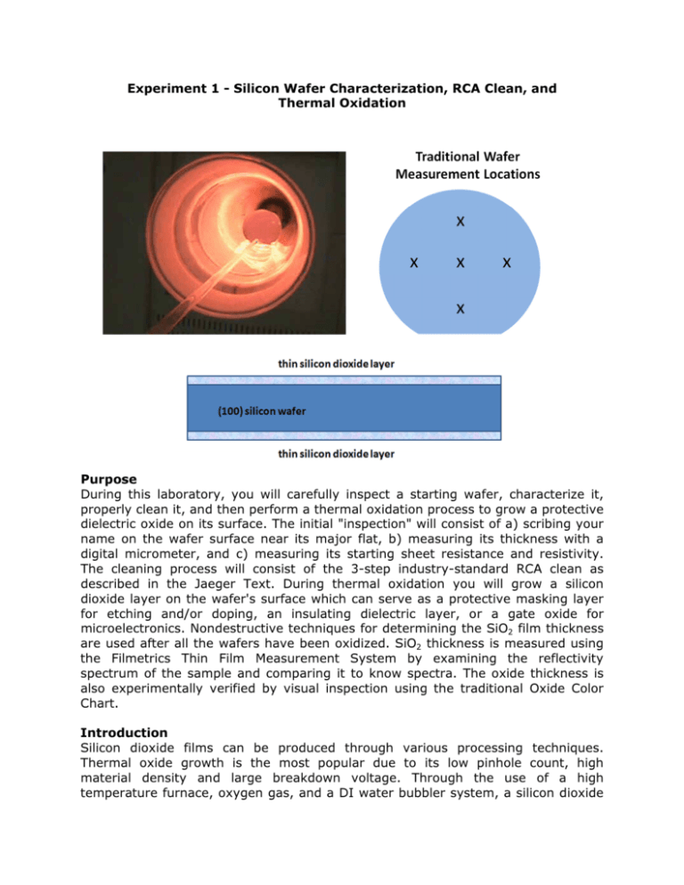
Experiment 1 - Silicon Wafer Characterization, RCA Clean, and Thermal Oxidation Purpose During this laboratory, you will carefully inspect a starting wafer, characterize it, properly clean it, and then perform a thermal oxidation process to grow a protective dielectric oxide on its surface. The initial "inspection" will consist of a) scribing your name on the wafer surface near its major flat, b) measuring its thickness with a digital micrometer, and c) measuring its starting sheet resistance and resistivity. The cleaning process will consist of the 3-step industry-standard RCA clean as described in the Jaeger Text. During thermal oxidation you will grow a silicon dioxide layer on the wafer's surface which can serve as a protective masking layer for etching and/or doping, an insulating dielectric layer, or a gate oxide for microelectronics. Nondestructive techniques for determining the SiO2 film thickness are used after all the wafers have been oxidized. SiO2 thickness is measured using the Filmetrics Thin Film Measurement System by examining the reflectivity spectrum of the sample and comparing it to know spectra. The oxide thickness is also experimentally verified by visual inspection using the traditional Oxide Color Chart. Introduction Silicon dioxide films can be produced through various processing techniques. Thermal oxide growth is the most popular due to its low pinhole count, high material density and large breakdown voltage. Through the use of a high temperature furnace, oxygen gas, and a DI water bubbler system, a silicon dioxide layer will be produced to a specified thickness. To estimate the thickness that will be produced, oxide growth charts and/or oxide modeling equations can be implemented. Once the oxide is grown, it can be used as a barrier to mask diffusions and/or ion implantations, act as a barrier to certain etchants, become a future MEMS bridge or cantilever structure, or function as a dielectric for a microelectronic device such as a capacitor or MOSFET. In this experiment, we will grow 500 nm of silicon dioxide to function as a protective masking layer against boron ion implantation (subsequent lab). Equipment Digital Micrometer Veeco 4-Point Probe RCA Benches Thermal Oxidation System Filmetrics Measurement System Materials and Supplies (100) DSP Silicon Wafers Diamond Scribe Wafer Tweezers Boat Holder and Push Rod Gases - Oxygen and Nitrogen SOPS (https://louisville.edu/research/cleanroom/sops) RCA Initial Wafer Clean Veeco 4-Point Probe Measurement System Thermal Oxidation Filmetrics Measurement System PRE_LAB ASSIGNMENT AND QUESTIONS (answer questions in your Lab Notebook and then submit a photo-copy to the TA at the start of this Lab) 1. Read the following material from Jaeger's "Introduction to Microelectronc Fabrication" - Silicon Wafer Cleaning Procedure (page 21) - Chapter 3 on Thermal Oxidation (pages 43-66) 2. Carefully review and print out the following Standard Operating Procedures (SOPs) - RCA Initial Wafer Clean - Veeco 4-Point Probe Measurement System - Thermal Oxidation - Filmetrics Measurement System 3. Using the Oxidation Charts found in Jaeger, determine the time required to grow 500 nm of silicon dioxide on a (100) silicon wafer under the following conditions: a) completely dry oxidation at 1000°C b) completely wet at 1000°C c) completely wet at 900°C d) completely wet at 1200°C 4. Determine the color of 500nm of silicon dioxide using the Color Chart found in Jaeger. 5. Determine the time it will take to etch 500 nm of silicon dioxide assuming you are using a Buffered Oxide Etching solution which nominally etches SiO2 at the rate of 1000 nm/min. LAB PROCEDURES (make comments and observations in your Lab Notebook) 1. Follow the "Bunny Suit Dressing Procedure" and enter the Cleanroom with the TA. 2. Using a diamond pencil scribe, carefully scribe your last name near the major flat on the backside of your (100) silicon wafer. If you are using a DSP (double side polished) wafer, select either side. Watch the TA and then follow his/her instructions. 2. Using the Digital Micrometer, carefully measure the thickness of your silicon wafer in four locations along its perimeter. Compare with the information on the Wafer box. Record results in your Lab Notebook. 3. Using the Veeco 4-Point Probe System, carefully measure the sheet resistance of your wafer in 5 locations (1 in the center and 4 along its perimeter). Convert to resistivity (ohm-cm) using either the settings of the Veeco or the definition of Sheet Resistance, which is "Sheet Resistance is equal to Resistivity divided by Thickness). Compare with the information on the Wafer box. Record, compare and discuss in your Lab Notebook. 4. Place your wafer in the RCA Cleaning Cassette along with the other class wafers. NOTE: Do not use metal tweezers. Use only the designated “RCA Cleaned” plastic tipped Tweezers while handling wafers for the RCA clean and thermal oxidation processes. 5. Perform an RCA clean as described in the Prelab SOP under the close observation of the TA. Note the difference between a hydrophilic and hydrophobic wafer surface. Discuss in your Lab Notebook. 6. Place your wafer in the Oxidation Wafer Boat along with the other class wafers. 7. Perform a Dry/Wet/Dry Thermal Oxidation for growing 500 nm of silicon dioxide. The dry oxidations are for only 12 minutes each. Their purpose is to surround the thick oxide with a thin dense film since dry oxidation produces a denser amorphous material than wet oxidation. Ignoring the thickness produced by the short dry oxidation steps, calculate the time needed to produce 500 nm of thermal oxide using wet oxidation at 1000°C. Record and discuss in your Lab Notebook. 8. Properly remove the wafer boat from the furnace (see SOP) and let the wafers cool to near-ambient temperature at the mouth of the furnace. 9. Remove your wafer from the wafer boat and determine the silicon dioxide thickness by using the Oxide Color Chart. Make sure you use perpendicular fluorescent light when observing its color. Note the color in your Lab Notebook and compare with your expected result. Note the uniformity of your color. Are there any color bands? Draw a picture of your wafer illustrating your result. 10. Using the Filmetrics Measurement System, determine the thickness of your oxide in the five traditional locations around your wafer. Compare your results from Step 9. Did you do a good job with your predictions and results? POST-LAB ASSIGNMENT AND QUESTIONS (answer questions in your Lab Notebook and then submit a photo-copy to the TA at the start of the next Lab) 1. Draw the Temperature vs. Time Profile for the program you used in this lab. 2. What gas(es) passes through the bubbler system during the oxidation process? At what temperature does the water need to be maintained? 3. What percent of the oxide growth is maintained above the original silicon surface? What percent of the oxide growth is below the original silicon surface? 4. What would happen to the oxidation rate at a given temperature if the pressure in the furnace could be increased? 5. If a wafer exhibits color bands after oxidation, what is that an indication of? Revised Aug 20, 2012 by KW, JA and DR
