Experiment_4
advertisement
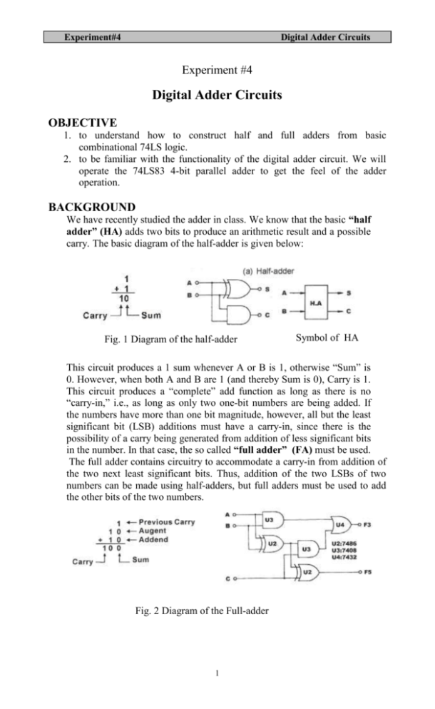
Experiment#4 Digital Adder Circuits Experiment #4 Digital Adder Circuits OBJECTIVE 1. to understand how to construct half and full adders from basic combinational 74LS logic. 2. to be familiar with the functionality of the digital adder circuit. We will operate the 74LS83 4-bit parallel adder to get the feel of the adder operation. BACKGROUND We have recently studied the adder in class. We know that the basic “half adder” (HA) adds two bits to produce an arithmetic result and a possible carry. The basic diagram of the half-adder is given below: Fig. 1 Diagram of the half-adder Symbol of HA This circuit produces a 1 sum whenever A or B is 1, otherwise “Sum” is 0. However, when both A and B are 1 (and thereby Sum is 0), Carry is 1. This circuit produces a “complete” add function as long as there is no “carry-in,” i.e., as long as only two one-bit numbers are being added. If the numbers have more than one bit magnitude, however, all but the least significant bit (LSB) additions must have a carry-in, since there is the possibility of a carry being generated from addition of less significant bits in the number. In that case, the so called “full adder” (FA) must be used. The full adder contains circuitry to accommodate a carry-in from addition of the two next least significant bits. Thus, addition of the two LSBs of two numbers can be made using half-adders, but full adders must be used to add the other bits of the two numbers. Fig. 2 Diagram of the Full-adder 1 Experiment#4 Digital Adder Circuits “Full-Adder” (FA) can be build using two half adders as shown in the figure below Symbol of FA Fig. 3 Full-adder using two HA To perform additions of numbers greater than 2-bits in length, the connection shown in Fig. 4, or “Parallel Adder” should be used to generate sums simultaneously. When FA1 adds Al and B1, a sum S1 and a carry C1 is generated. Cl will be added to A2 and B2 by FA2, generating another sum S2 and another carry C2, and so on. The 7483 is a four bit binary parallel adder IC you can obtain its pin diagram from data sheets given online. Fig. 4 four bit binary parallel adder Fig. 4 Pin diagram of 74LS83 IC. 2 Experiment#4 Digital Adder Circuits PRELAB: 1. Draw pin diagram and truth table for HA circuit shown in fig.1. 2. Draw pin diagram and truth table for FA circuit shown in fig.2. EQUIPMENTS REQUIRED KL-31001 trainer kit, lab module KL-33004, and 7483(binary adder). PROCEDURES: Part I: a) Construct the circuit of HA using module KL-33004 block a, connect inputs A and B to data switches and outputs F1 (carry) and F2 (sum) to LEDs, and do any other connections using clips. Record the truth table of the circuit and compare with that in your prelab. Part II: a) Construct the circuit of FA using module KL-33004 block a, connect inputs A, B and C to data switches and outputs F3 (carry) and F5 (sum) to LEDs. and do any other connections using clips Record the truth table of the circuit and compare with that in your prelab. Part III: Parallel-Adder Circuit with IC a) Use the IC 7483 to add binary numbers A and B. b) Connect inputs A0A3 (addends), B0B3 (augends) to DIP Switches DIP2: O3 and DIP1:03 respectively. Connect ΣO, Σ1, Σ2, Σ3 , C4 to LEDs L1L5. Follow input sequences in Table 1, record C4 and sum in hexadecimal numbers. 3 Experiment#4 Digital Adder Circuits Y 0 0 0 0 0 1 1 1 3 4 4 8 9 A C F X 0 1 6 9 F 3 6 8 6 8 F 7 9 B E F Σ F1 (carry) Table 1 Exercises: a. Construct half subtractor circuit. Show logic diagram and schematic diagram. b. Connect two 7483 ICs to add two binary numbers each of 8 bit. Show schematic diagram. 4
