Abstract Template
advertisement
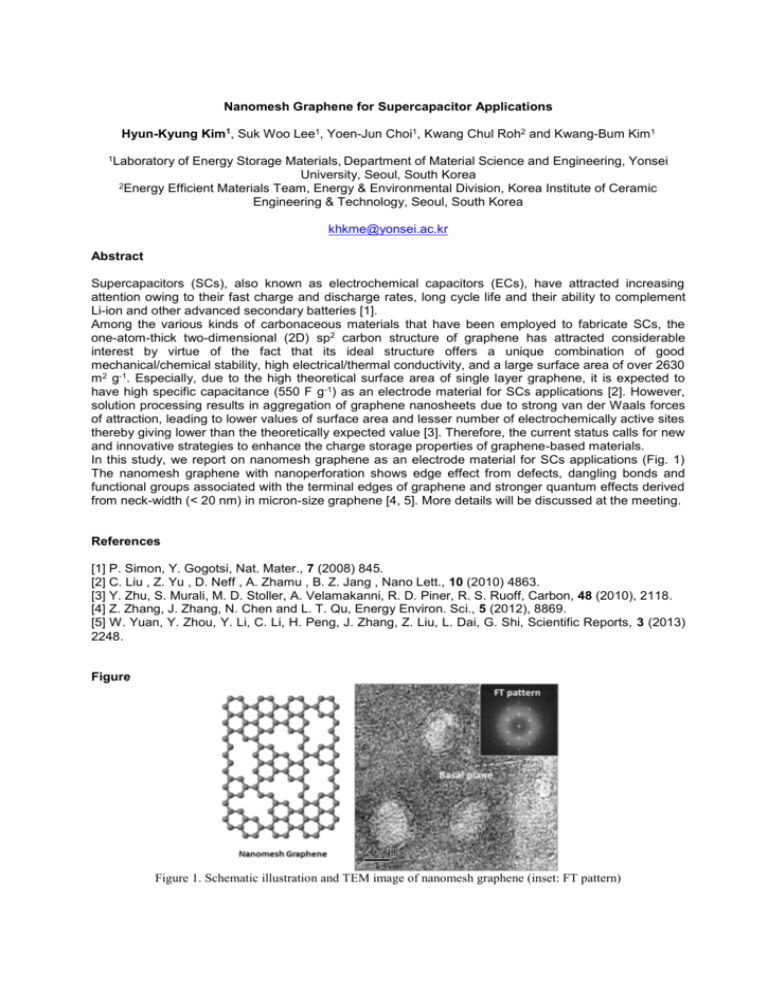
Nanomesh Graphene for Supercapacitor Applications Hyun-Kyung Kim1, Suk Woo Lee1, Yoen-Jun Choi1, Kwang Chul Roh2 and Kwang-Bum Kim1 1Laboratory of Energy Storage Materials, Department of Material Science and Engineering, Yonsei University, Seoul, South Korea 2Energy Efficient Materials Team, Energy & Environmental Division, Korea Institute of Ceramic Engineering & Technology, Seoul, South Korea khkme@yonsei.ac.kr Abstract Supercapacitors (SCs), also known as electrochemical capacitors (ECs), have attracted increasing attention owing to their fast charge and discharge rates, long cycle life and their ability to complement Li-ion and other advanced secondary batteries [1]. Among the various kinds of carbonaceous materials that have been employed to fabricate SCs, the one-atom-thick two-dimensional (2D) sp2 carbon structure of graphene has attracted considerable interest by virtue of the fact that its ideal structure offers a unique combination of good mechanical/chemical stability, high electrical/thermal conductivity, and a large surface area of over 2630 m2 g-1. Especially, due to the high theoretical surface area of single layer graphene, it is expected to have high specific capacitance (550 F g-1) as an electrode material for SCs applications [2]. However, solution processing results in aggregation of graphene nanosheets due to strong van der Waals forces of attraction, leading to lower values of surface area and lesser number of electrochemically active sites thereby giving lower than the theoretically expected value [3]. Therefore, the current status calls for new and innovative strategies to enhance the charge storage properties of graphene-based materials. In this study, we report on nanomesh graphene as an electrode material for SCs applications (Fig. 1) The nanomesh graphene with nanoperforation shows edge effect from defects, dangling bonds and functional groups associated with the terminal edges of graphene and stronger quantum effects derived from neck-width (< 20 nm) in micron-size graphene [4, 5]. More details will be discussed at the meeting. References [1] P. Simon, Y. Gogotsi, Nat. Mater., 7 (2008) 845. [2] C. Liu , Z. Yu , D. Neff , A. Zhamu , B. Z. Jang , Nano Lett., 10 (2010) 4863. [3] Y. Zhu, S. Murali, M. D. Stoller, A. Velamakanni, R. D. Piner, R. S. Ruoff, Carbon, 48 (2010), 2118. [4] Z. Zhang, J. Zhang, N. Chen and L. T. Qu, Energy Environ. Sci., 5 (2012), 8869. [5] W. Yuan, Y. Zhou, Y. Li, C. Li, H. Peng, J. Zhang, Z. Liu, L. Dai, G. Shi, Scientific Reports, 3 (2013) 2248. Figure Figure 1. Schematic illustration and TEM image of nanomesh graphene (inset: FT pattern)
