Supplementary information (docx 8789K)
advertisement
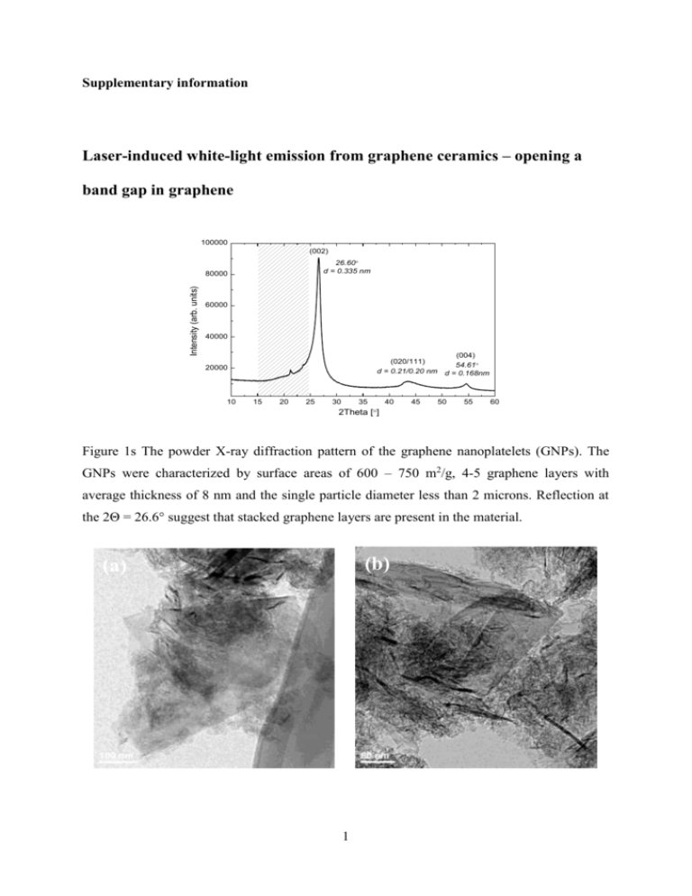
Supplementary information Laser-induced white-light emission from graphene ceramics – opening a band gap in graphene 100000 (002) 26.60 d = 0.335 nm Intensity (arb. units) 80000 60000 40000 (004) (020/111) 54.61 d = 0.21/0.20 nm d = 0.168nm 20000 10 15 20 25 30 35 40 45 50 55 60 2Theta [] Figure 1s The powder X-ray diffraction pattern of the graphene nanoplatelets (GNPs). The GNPs were characterized by surface areas of 600 – 750 m2/g, 4-5 graphene layers with average thickness of 8 nm and the single particle diameter less than 2 microns. Reflection at the 2Θ = 26.6° suggest that stacked graphene layers are present in the material. (b) (a) 1 Figure 2s Representative images of graphene nanoplatelets acquired via transmission electron microscopy (TEM). Graphene plates and some carbonaceous amorphous phase can be clearly observed. Figure 3s SEM images of a graphene green body (a) and a ceramic (b) sintered at 8 GPa and 500°C. There are visible differences between the cold-pressed (green body) and sintered ceramics. After pressing, the number of pores and their sizes significantly decreased, and the ceramic became consolidated with a much smoother surface. A representative image of a graphene ceramic sample is presented as an inset in Figure 3b. 2 Figure 4s The CIE 1931 chromaticity coordinates calculated for the graphene ceramics after excitation at various photon energies: (a) 2.6 eV (476 nm), (b) 2.5 eV (488 nm), (c) 2.4 eV (514 nm), (d) 1.5 eV (808) nm and (e) 1.2 eV (976 nm). 3

