Supplemental online material
The effect of size on dislocation cell formation and strain hardening in aluminium
Qian Yu a,b
, Raja K. Mishra c
, John W. Morris Jr a and Andrew M. Minor a,b
* a
Department of Materials Science and Engineering, University of California, Berkeley, CA, USA; b
The National Center for Electron Microscopy, Lawrence Berkeley National Laboratory, Berkeley,
CA, USA; c
General Motors Research and Development Center, Warren, WI, USA
1) Sample preparation
Supplemental online material
Micron-sized specimens were fabricated with a FEI Strata 235 Dual Beam Focus Ion
Beam (FIB). Before FIB milling process, an Al foil was cut out from a single crystal
Al rod. One of the edges of the thin Al foil was required to be parallel to [001]. This piece of Al was further mechanically milled to about 50 micron thick. Ion milling was then used on the thin Al foil in a Gatan Precision Ion Polishing System (PIPS), which has 2 unique penning ion guns with 10° to -10° milling angles and liquid nitrogen specimen cooling. The beam was centered at the edge of the thin foil, which was normal to [001] direction. The ion milling process was carried under electron beam with energy at 200 eV for about 1 hour. As the next step, the thin foil was further glued to an in situ TEM copper stage using colloidal graphite. The TEM stage was then glued to a 45 degree SEM stage. The whole was installed into FIB and the chamber was pumped down to 10
-5
torr vacuum for operation. Since the angle between ion beam and electron beam in FIB is 52 degree, we firstly tilted the stage by 7 degree, so that the ion beam direction was perpendicular to the edge of the thin foil. FIBmilling process was performed in the sequence of rough cutting with 5000 pA ion beam current and finer cutting with 100 pA ion beam current. These would produce a thinner window with thickness at about 1 micron. Afterwards, the stage was rotated by
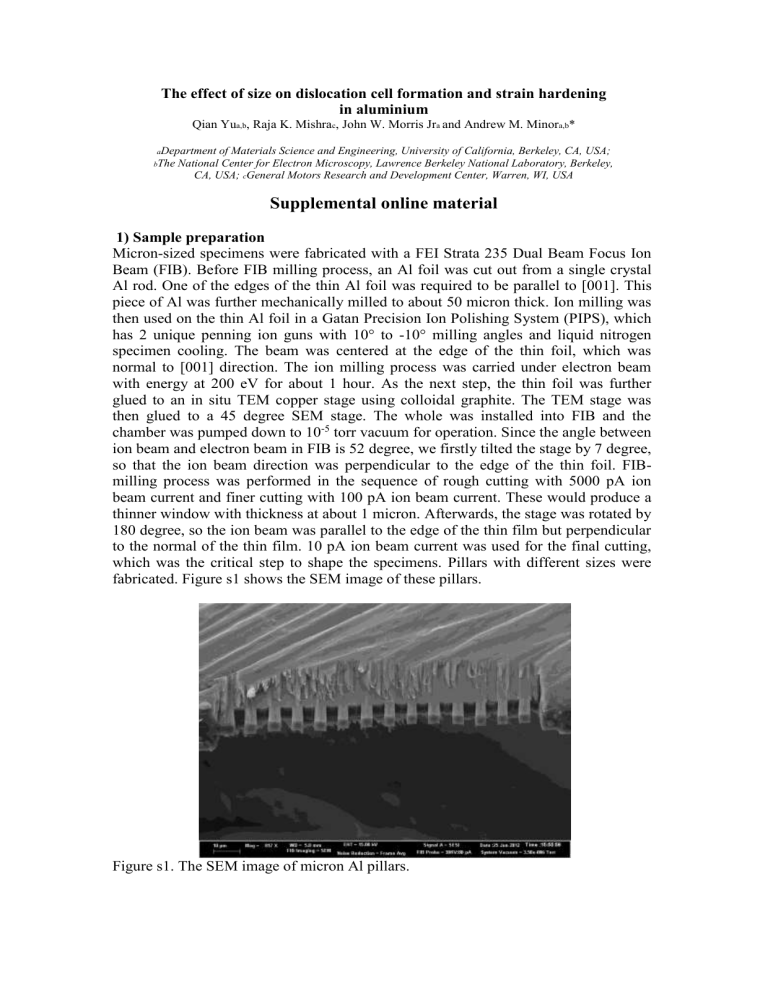
180 degree, so the ion beam was parallel to the edge of the thin film but perpendicular to the normal of the thin film. 10 pA ion beam current was used for the final cutting, which was the critical step to shape the specimens. Pillars with different sizes were fabricated. Figure s1 shows the SEM image of these pillars.
Figure s1. The SEM image of micron Al pillars.
All of the TEM samples were sectioned from the deformed samples in the same manner, as shown in Figure S2. The angle between the normal of the TEM foils and the loading direction was the same for all of the pillars. The foil was glued onto a 45 degree SEM stub and was further tilted to 30 degree. The Focused Ion Beam with current at 10 pA was used to slice the TEM cross-section samples from the micron pillars from the top-down. This geometry resulted in the largest possible cross-section for TEM analysis from each pillar.
Figure S2. Schematic of the TEM sample preparation, showing the orientation of the
TEM sections with respect to the pillar geometry.
