Adders
advertisement
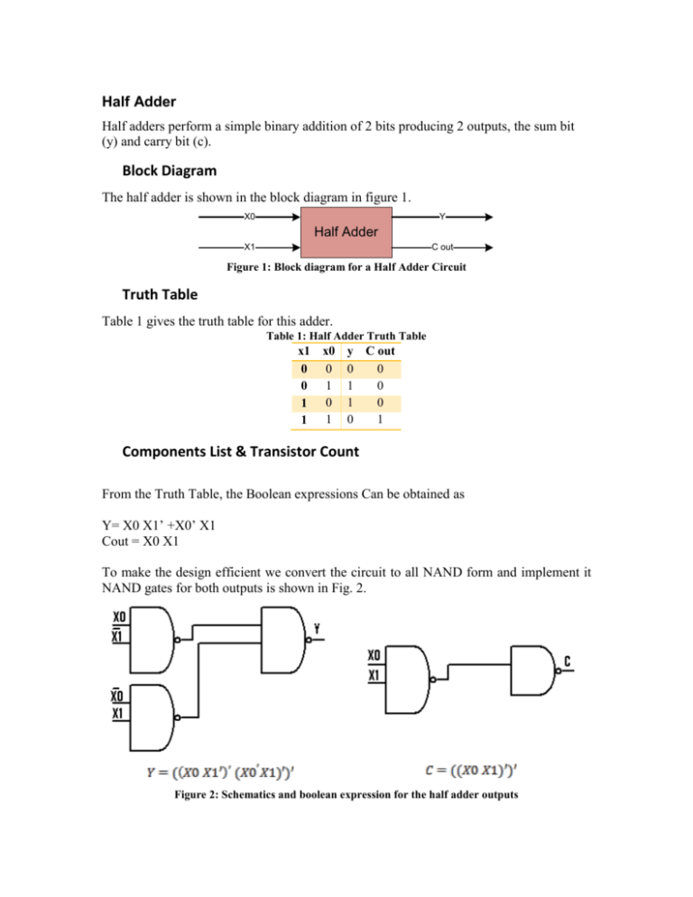
Half Adder Half adders perform a simple binary addition of 2 bits producing 2 outputs, the sum bit (y) and carry bit (c). Block Diagram The half adder is shown in the block diagram in figure 1. X0 Y Half Adder X1 C out Figure 1: Block diagram for a Half Adder Circuit Truth Table Table 1 gives the truth table for this adder. Table 1: Half Adder Truth Table x1 x0 y C out 0 0 0 0 0 0 1 1 0 1 0 1 1 1 1 0 Components List & Transistor Count From the Truth Table, the Boolean expressions Can be obtained as Y= X0 X1’ +X0’ X1 Cout = X0 X1 To make the design efficient we convert the circuit to all NAND form and implement it NAND gates for both outputs is shown in Fig. 2. Figure 2: Schematics and boolean expression for the half adder outputs Simulation Full Adder The full adder block diagram is shown in Fig. 3. X0 X1 S Full Adder C in C out Figure 3: Block diagram for a Full Adder Circuit Truth Table Table 2 gives the truth table for this adder. Table 2: Full Adder Truth Table C in x1 x0 S C out 0 0 0 0 0 0 1 1 0 0 1 0 1 0 0 1 1 0 1 0 0 0 1 0 1 0 1 0 1 1 1 0 0 1 1 1 1 1 1 1 Schematics and Boolean Expression From the Truth Table, the Boolean expressions is given as: using NAND gates the circuit can be implemented as shown in Fig. 4 Figure 4 Schematics and Boolean expression for the full adder outputs Figure 5 Full adder simulation results Using simple logic design and minimization techniques we can derive the following formula for the single bit full adder. Sum = (A XOR B) XOR Cin Cout =A . B + Cin . (A XOR B) Circuit implementation is shown in Fig. 6 6 Fig. 6 Alternative implementation of One bit Full Adder Logic Design 3.1 Adder architecture overview A n-bit binary adder can be seen as the special arrangement of n full adder units that each take three one-bit inputs: A, B and carry Ci and which generate sum S and carry out Co, as shown in Figure 1. The expression for S and Co can be given as: Figure 3.1: 1-bit Full adder and its truth table The characteristics of a few common adder architectures are summarized in the following subsections, which include: Ripple Carry Adder (RCA), Carry Bypass Adder (CBA), Carry Select (CS), CCS, CSA, and CLA. 3.1.1 Ripple Carry Adder (RCA) An n-bit Ripple Carry Adder (RCA) is a simple cascading of n full adders as shown in Figure 2. In the RCA, the carry bit ripples from one stage of the adder chain to the next. Figure 3.2: Ripple carry adder architecture The worst-case delay of the RCA is when a carry signal transition ripples through all stages of adder chain from the least significant bit to the most significant bit, which is approximated by: where tc is the delay through the carry stage of a full adder, and ts is the delay to compute the sum of the last stage. The delay of ripple carry adder is linearly proportional to n, the number of bits, therefore the performance of the RCA is limited when n grows bigger. The advantages of the RCA are lower power consumption as well as a compact layout giving smaller chip area. 3.1.4 Carry Lookahead Adder (CLA) The CLA removes the carry-ripple effect in the other types of adders described above. The architecture of a CLA is shown in Figure 5. Since the CLA generates a carry for each bit simultaneously, the delay is greatly reduced. The independent carry can be computed by expanding from equation 4: In practice, it is not possible to use the CLA to realize constant delay for the wider-bit adders since there will be a substantial loading capacitance, and hence larger delay and larger power consumption. The CLA has the fastest growing area requirements with respect to the bit size. Figure 3.1: CLA architecture In practice, the mixture of architectures listed above are often used in the design of wider bit adders to realize better optimization in terms of design metrics such as performance, power consumption, Power-delay Product (PDP), Energy-delay Product (EDP), area, and noise margin, etc. One Bit Full Adder: The main objective of this phase is to get a logically minimized expression to evaluate the two required output from the three inputs of the single bit full adder. First the main functionality of the single bit adder can be modeled by the following table (see table1) Table 2One Bit Full Adder Truth Table A B CIN SUM COUT 0 0 0 0 0 0 0 1 1 0 0 1 0 1 0 0 1 1 0 1 1 0 0 1 0 1 0 1 0 1 1 1 0 0 1 1 1 1 1 1 Using simple logic design and minimization techniques we can derive the following formula for our single bit full adder. Sum = (A XOR B) XOR Cin Cout =A . B + Cin . (A XOR B) See figure1 for the gate implementation of this equation. Figure 2One bit Full Adder Logic Design We can see clearly from figure 1 that the critical path is the path from the input to the COUT. This gives us a clue for the path that we have to optimize during the circuit design phase. We have used (Logic Works version 4.01) to logically simulate the functionality of this adder. We applied the 8 test vectors shown above and ran the simulation for enough time. Finally we got the results witch matched the ones in table1 Four Bit Full Adder: Here is an important decision point which is affecting our design criteria. We need to choose the type of adder and the type of carry propagation we are going to use. There are two main categories of adders. Carry Look Ahead Adders and Carry Ripple Adders Ripple Carry Adder In this type of adders, the output carry from one block is connected to the carry input pin of the next block. So the carry will propagate serially through full adder blocks (see figure2). The main advantage of this approach is its ease of implementation (modularity) but it cost more delay since the critical path length now is proportional to the size of the adder (number of bits) (see figure2) critical path is in red color. Figure 3Ripple Carry Adder (Logical Design) Carry Look Ahead adder Carry look ahead adder depends on the idea of generating and propagating the carry. However the maximum delay for the curry now is 2 logic levels. See figure 3 and figure 4 for details. Figure 4Carry Look Ahead Adder (Logical design) Where G, P and carry values are as follows Gi = Ai.Bi Pi = (Ai Bi) C1 = G0 + P0.C0 C2 = G1 + P1.C1 = G1 + P1.G0 + P1.P0.C0 C3 = G2 + P2.G1 + P2.P1.G0 + P2.P1.P0.C0 C4 = G3 + P3.G2 + P3.P2.G1 + P3P2.P1.G0 + P3P2.P1.P0.C0 It is clear that the main advantage of Carry look a head adder is the delay reduction due to the Carry Look Ahead logic block. However it increases the area significantly as the number of bits increases . Some other adder implementations also exists where different combinations of ripple and look ahead and other logic blocks are used.
