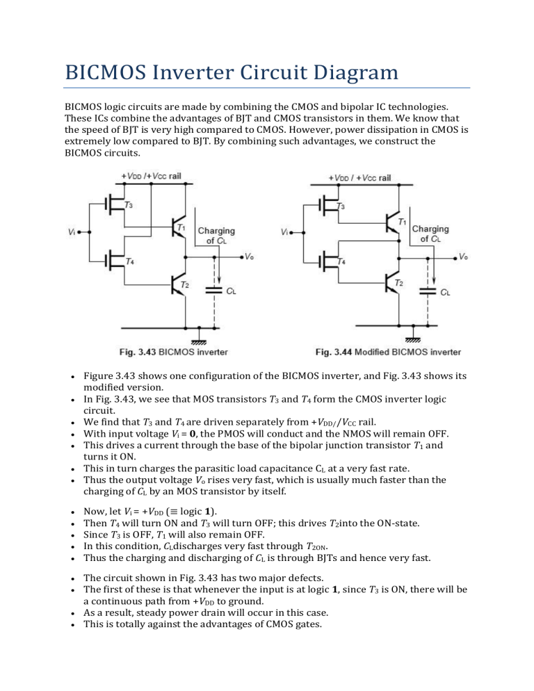
BICMOS Inverter Circuit Diagram BICMOS logic circuits are made by combining the CMOS and bipolar IC technologies. These ICs combine the advantages of BJT and CMOS transistors in them. We know that the speed of BJT is very high compared to CMOS. However, power dissipation in CMOS is extremely low compared to BJT. By combining such advantages, we construct the BICMOS circuits. Figure 3.43 shows one configuration of the BICMOS inverter, and Fig. 3.43 shows its modified version. In Fig. 3.43, we see that MOS transistors T3 and T4 form the CMOS inverter logic circuit. We find that T3 and T4 are driven separately from +VDD//VCC rail. With input voltage Vi = 0, the PMOS will conduct and the NMOS will remain OFF. This drives a current through the base of the bipolar junction transistor T1 and turns it ON. This in turn charges the parasitic load capacitance CL at a very fast rate. Thus the output voltage Vo rises very fast, which is usually much faster than the charging of CL by an MOS transistor by itself. Now, let Vi = +VDD (≡ logic 1). Then T4 will turn ON and T3 will turn OFF; this drives T2into the ON-state. Since T3 is OFF, T1 will also remain OFF. In this condition, CLdischarges very fast through T2ON. Thus the charging and discharging of CL is through BJTs and hence very fast. The circuit shown in Fig. 3.43 has two major defects. The first of these is that whenever the input is at logic 1, since T3 is ON, there will be a continuous path from +VDD to ground. As a result, steady power drain will occur in this case. This is totally against the advantages of CMOS gates. The second defect is that there is no discharge path for the base currents of T1 and T2. This will therefore reduce the speed of the circuit. To overcome these problems, we modify the circuit, as shown in Fig. 3.44. In this case, NMOS transistor T4 has its drain connected to the output terminal rather than to +VDD. As before, when T3 is turned ON, T1 is also turned ON. Now, when T4 is turned ON, we find T2 also to turn ON.. However, since the collector and base of T2 are shorted together through T4ON, the output voltage Vo will now be equal VBES, the saturation base-emitter voltage of T2 (= 0.8 V). Thus in this case, the output swing is between VCC and VBES.
