CSE 493/593 Fall 2015 Homework 1 Due: 6:30pm Oct 21
advertisement
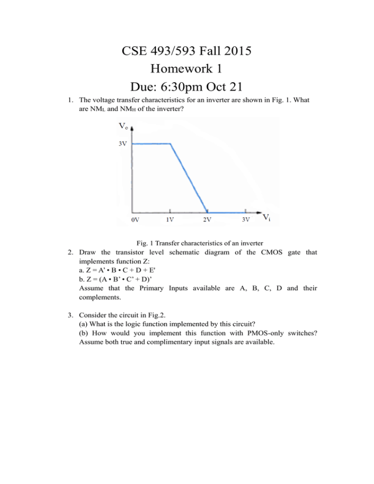
CSE 493/593 Fall 2015 Homework 1 Due: 6:30pm Oct 21 1. The voltage transfer characteristics for an inverter are shown in Fig. 1. What are NML and NMH of the inverter? Fig. 1 Transfer characteristics of an inverter 2. Draw the transistor level schematic diagram of the CMOS gate that implements function Z: a. Z = A’ • B • C + D + E' b. Z = (A • B’ • C’ + D)’ Assume that the Primary Inputs available are A, B, C, D and their complements. 3. Consider the circuit in Fig.2. (a) What is the logic function implemented by this circuit? (b) How would you implement this function with PMOS-only switches? Assume both true and complimentary input signals are available. Fig. 2 Circuit 4. Assume inputs and its complements are available. If a Boolean function is D = A′BC + AB′C + AC′ + B′C′ , then: (a) Implement the function using transmission gate and draw the transistor level schematic diagram. (b) Implement this function using a compound CMOS gate and draw the transistor level schematic diagram.
