TIM7179-4UL
advertisement
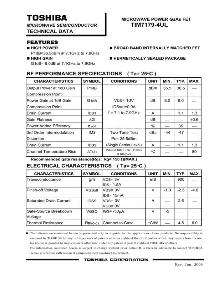
MICROWAVE POWER GaAs FET TIM7179-4UL MICROWAVE SEMICONDUCTOR TECHNICAL DATA FEATURES HIGH POWER P1dB=36.5dBm at 7.1GHz to 7.9GHz HIGH GAIN G1dB= 9.0dB at 7.1GHz to 7.9GHz BROAD BAND INTERNALLY MATCHED FET HERMETICALLY SEALED PACKAGE RF PERFORMANCE SPECIFICATIONS CHARACTERISTICS Output Power at 1dB Gain SYMBOL ( Ta= 25°C ) CONDITIONS P1dB UNIT MIN. TYP. MAX. dBm 35.5 36.5 ⎯ dB 8.0 9.0 ⎯ A ⎯ 1.1 1.3 Compression Point Power Gain at 1dB Gain VDS= 10V G1dB Compression Point IDSset=0.9A f = 7.1 to 7.9GHz Drain Current IDS1 Gain Flatness ΔG dB ⎯ ⎯ ±0.6 Power Added Efficiency ηadd % ⎯ 35 ⎯ 3rd Order Intermodulation IM3 dBc -44 -47 ⎯ Distortion Drain Current Channel Temperature Rise Two-Tone Test Po= 25.5dBm IDS2 (Single Carrier Level) A ⎯ 1.1 1.3 ΔTch (VDS X IDS + Pin – P1dB) °C ⎯ ⎯ 80 UNIT mS MIN. V -1.0 -2.5 -4.0 A ⎯ 2.6 ⎯ V -5 ⎯ ⎯ °C/W ⎯ 4.5 6.0 X Rth(c-c) Recommended gate resistance(Rg) : Rg= 150 Ω(MAX.) ELECTRICAL CHARACTERISTICS CHARACTERISTICS Transconductance Pinch-off Voltage SYMBOL gm VGSoff Saturated Drain Current IDSS Gate-Source Breakdown Voltage VGSO Thermal Resistance ( Ta= 25°C ) CONDITIONS VDS= 3V IDS= 1.5A VDS= 3V IDS= 15mA VDS= 3V VGS= 0V IGS= -50μA Rth(c-c) Channel to Case ⎯ TYP. MAX. 900 ⎯ The information contained herein is presented only as a guide for the applications of our products. No responsibility is assumed by TOSHIBA for any infringements of patents or other rights of the third parties which may results from its use, No license is granted by implication or otherwise under any patent or patent rights of TOSHIBA or others. The information contained herein is subject to change without prior notice. It is therefor advisable to contact TOSHIBA before proceeding with design of equipment incorporating this product. Rev. Jun. 2009 TIM7179-4UL ABSOLUTE MAXIMUM RATINGS ( Ta= 25°C ) CHARACTERISTICS SYMBOL UNIT RATING Drain-Source Voltage VDS V 15 Gate-Source Voltage VGS V -5 Drain Current IDS A 3.5 Total Power Dissipation (Tc= 25 °C) PT W 25 Channel Temperature Tch °C 175 Storage Tstg °C -65 to +175 PACKAGE OUTLINE (2-11D1B) Unit in mm c Gate d Source e Drain HANDLING PRECAUTIONS FOR PACKAGE MODEL Soldering iron should be grounded and the operating time should not exceed 10 seconds at 260°C. 2 TIM7179-4UL RF PERFORMANCE Output Power vs. Frequency 39 VDS= 10V IDS≅ 1.1A Pin= 27.5dBm 37 36 35 34 6.8 7 7.2 7.4 7.6 7.8 8 8.2 Frequency (GHz) Output Power vs. Input Power 90 f= 7.5GHz VDS= 10V IDS≅ 1.1A 39 80 38 70 Po 37 60 36 50 ηadd 35 40 34 30 33 20 32 10 31 0 21 23 25 27 Pin (dBm) 3 29 31 ηadd (%) 40 Po (dBm) Po (dBm) 38 TIM7179-4UL Power Dissipation vs. Case Temperature 30 P T (W) 20 10 0 0 40 80 1 20 16 0 20 0 Tc (℃) IM3 vs. Output Power Characteristics -20 VDS= 10V IDS≅ 1.1A f= 7.5GHz Δf= 5MHz IM3 (dBc) -30 -40 -50 -60 21 23 25 27 29 Po(dBm), Single Carrier Level 4 31

