(iv) Operation as vDS Is Increased • As we travel along the channel
advertisement
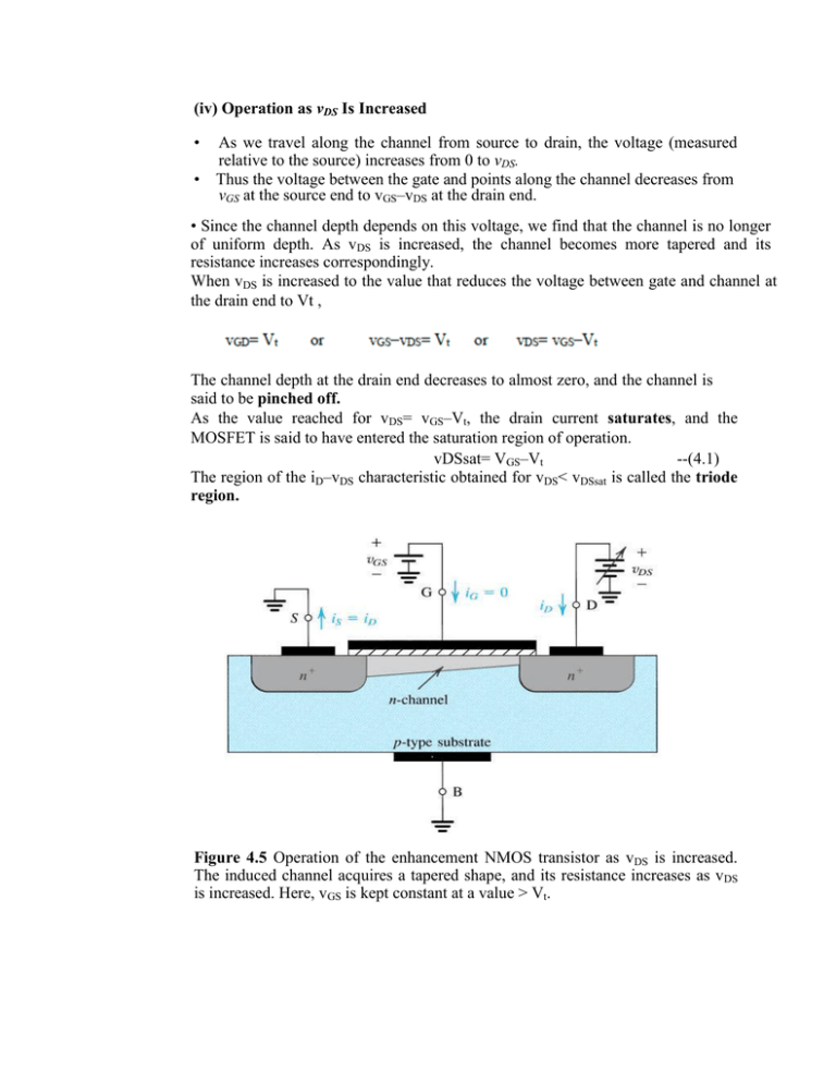
(iv) Operation as vDS Is Increased • As we travel along the channel from source to drain, the voltage (measured relative to the source) increases from 0 to vDS. • Thus the voltage between the gate and points along the channel decreases from vGS at the source end to vGS–vDS at the drain end. • Since the channel depth depends on this voltage, we find that the channel is no longer of uniform depth. As vDS is increased, the channel becomes more tapered and its resistance increases correspondingly. When vDS is increased to the value that reduces the voltage between gate and channel at the drain end to Vt , The channel depth at the drain end decreases to almost zero, and the channel is said to be pinched off. As the value reached for vDS= vGS–Vt, the drain current saturates, and the MOSFET is said to have entered the saturation region of operation. vDSsat= VGS–Vt --(4.1) The region of the iD–vDS characteristic obtained for vDS< vDSsat is called the triode region. Figure 4.5 Operation of the enhancement NMOS transistor as vDS is increased. The induced channel acquires a tapered shape, and its resistance increases as vDS is increased. Here, vGS is kept constant at a value > Vt. Derivation of the iD-vDS Relationship In the MOSFET, the gate and the channel region form a parallel-plate capacitor for which the oxide layer serves as a dielectric. Figure 4.7 Derivation of the iD-vDS Relationship of the NMOS transistor If the capacitance per unit gate area is denoted Cox and the thickness of the oxide layer is tox, then Cox=εox/ tox (4.2) Where εox is the permittivity of the silicon oxide, ε= 3.9 ε0= 3.9×8.854×10-12 3.45×10⁻¹¹F/m 4.1.7 The p-Channel MOSFET A p-channel enhancement-type MOSFET (PMOS transistor), fabricated on an n-type substrate with p+ regions for the drain and source, has holes as charge carriers. The device operates in the same manner as the n-channel device except that vGS and vDS are negative and the threshold voltage Vt is negative. Also, the current i D enters the source terminal and leaves through the drain terminal. Figure 4.8 Physical construction of p channel E-MOSFET In general, NMOS devices are normally preferred to PMOS because Smaller Operate faster and Requires lower supply voltages than PMOS. 4.1.7 Complementary MOS or CMOS As the name implies, complementary MOS technology employs MOS transistors of both polarities. At present time CMOS is the most widely used of all the IC technologies. Figure 4.9 shows cross-section of a CMOS chip illustrating how the PMOS and NMOS transistors are fabricated. While the NMOS transistor is implemented directly in the p-type substrate, the PMOS transistor is fabricated in a specially created n region, known as an nwell. Figure 4.9 Cross-section of a CMOS integrated circuit. Not shown are the connections made to the p-type body and to the n well; the latter functions as the body terminal for the pchannel device.
