FET Temperature Effects
advertisement
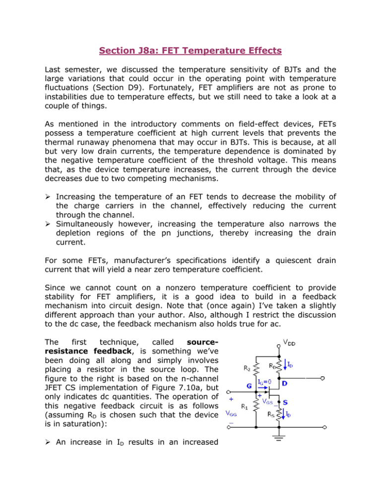
Section J8a: FET Temperature Effects Last semester, we discussed the temperature sensitivity of BJTs and the large variations that could occur in the operating point with temperature fluctuations (Section D9). Fortunately, FET amplifiers are not as prone to instabilities due to temperature effects, but we still need to take a look at a couple of things. As mentioned in the introductory comments on field-effect devices, FETs possess a temperature coefficient at high current levels that prevents the thermal runaway phenomena that may occur in BJTs. This is because, at all but very low drain currents, the temperature dependence is dominated by the negative temperature coefficient of the threshold voltage. This means that, as the device temperature increases, the current through the device decreases due to two competing mechanisms. ¾ Increasing the temperature of an FET tends to decrease the mobility of the charge carriers in the channel, effectively reducing the current through the channel. ¾ Simultaneously however, increasing the temperature also narrows the depletion regions of the pn junctions, thereby increasing the drain current. For some FETs, manufacturer’s specifications identify a quiescent drain current that will yield a near zero temperature coefficient. Since we cannot count on a nonzero temperature coefficient to provide stability for FET amplifiers, it is a good idea to build in a feedback mechanism into circuit design. Note that (once again) I’ve taken a slightly different approach than your author. Also, although I restrict the discussion to the dc case, the feedback mechanism also holds true for ac. The first technique, called sourceresistance feedback, is something we’ve been doing all along and simply involves placing a resistor in the source loop. The figure to the right is based on the n-channel JFET CS implementation of Figure 7.10a, but only indicates dc quantities. The operation of this negative feedback circuit is as follows (assuming RD is chosen such that the device is in saturation): ¾ An increase in ID results in an increased voltage drop across RS (↑VS). ¾ Since the voltage at the gate is constant (the Thevenin voltage, VGG), an increase in VS results in a corresponding decrease in VGS (VGS=VGG-VS). ¾ The decrease in VGS results in a decrease in ID (from the current equations), therefore indicating the presence of a negative feedback mechanism that tends to reduce the original change in drain current. Source-resistance feedback works for JFETs and all types of MOSFETs (and we used it for BJTs too). To increase the gain of the amplifier, part or all of RS may be bypassed with a capacitor. Your author also states that a typical value of RS that will provide a reasonable ID deviation is 10% of the value of RD. Another common biasing arrangement for enhancement type MOSFETs is called drainto-gate feedback. This strategy is shown in Figure 7.10b for an enhancement NMOS and a modified version is given to the right. This feedback mechanism involves a resistor (RG, usually large) connected between the gate and drain. Since the gate current may be considered zero for a MOSFET, the voltage at the drain is equal to the voltage at the gate for dc operation. Setting these two voltages equal ensures operation in the saturation region (refer to the MOSFET table in Section J3b). Operation of this circuit is as follows: ¾ If the drain current increases, the voltage drop across RD will also increase, resulting in a decrease of the voltage at the drain (↓VDS). ¾ Since VGS=VDS, the voltage at the gate will also decrease, resulting in a decrease in VGS. ¾ As in the previous feedback configuration, the decrease in VGS results in a decrease in ID. Once again, we have negative feedback that tends to reduce the original change in drain current.
