5N0
3
WFY
WFY5
N03
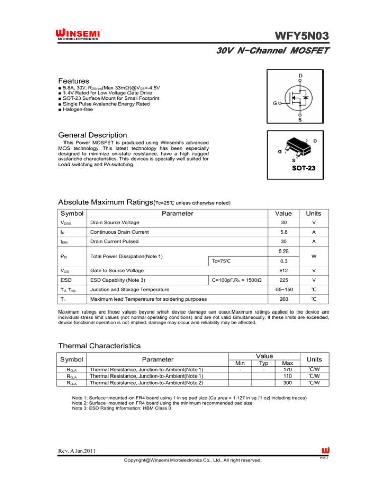
30V N−Channel MOSFET
Features
■ 5.8A, 30V, RDS(on)(Max 33mΩ)@VGS=-4.5V
■ 1.4V Rated for Low Voltage Gate Drive
■ SOT-23 Surface Mount for Small Footprint
■ Single Pulse Avalanche Energy Rated
■ Halogen-free
General Description
D
This Power MOSFET is produced using Winsemi’s advanced
MOS technology. This latest technology has been especially
designed to minimize on-state resistance, have a high rugged
avalanche characteristics. This devices is specially well suited for
Load switching and PA switching.
G
S
T-23
SO
SOT
Absolute Maximum Ratings(Tc=25℃ unless otherwise noted)
Symbol
Parameter
Value
Units
VDSS
Drain Source Voltage
30
V
ID
Continuous Drain Current
5.8
A
IDM
Drain Current Pulsed
30
A
PD
Total Power Dissipation(Note 1)
0.25
W
Tc=75℃
VGS
Gate to Source Voltage
ESD
ESD Capability (Note 3)
TJ, Tstg
Junction and Storage Temperature
TL
Maximum lead Temperature for soldering purposes
0.3
C=100pF,RS = 1500Ω
±12
V
225
V
-55~150
℃
260
℃
Maximum ratings are those values beyond which device damage can occur.Maximum ratings applied to the device are
individual stress limit values (not normal operating conditions) and are not valid simultaneously. If these limits are exceeded,
device functional operation is not implied, damage may occur and reliability may be affected.
Thermal Characteristics
Symbol
RQJA
RQJA
RQJA
Parameter
Thermal Resistance, Junction-to-Ambient(Note 1)
Thermal Resistance, Junction-to-Ambient(Note 1)
Thermal Resistance, Junction-to-Ambient(Note 2)
Value
Min
Typ
Max
-
-
170
110
300
Units
℃/W
℃/W
℃/W
Note 1: Surface−mounted on FR4 board using 1 in sq pad size (Cu area = 1.127 in sq [1 oz] including traces)
Note 2: Surface−mounted on FR4 board using the minimum recommended pad size.
Note 3: ESD Rating Information: HBM Class 0
Rev. A Jun.2011
Copyright@Winsemi Microelectronics Co., Ltd., All right reserved.
P03-3
5N0
3
WFY
WFY5
N03
Electrical Characteristics (Tc = 25°C)
Characteristics
Symbol
Test Condition
Min
Type
Max
Unit
Gate leakage current(Note 4)
IGSS
VGS = ±12 V, VDS = 0 V
-
-
±100
nA
Drain cut−off current(Note 4)
IDSS
VDS =24 V, VGS = 0 V
-
-
1
μA
V(BR)DSS
ID = 250 μA, VGS = 0 V
30
-
-
V
Gate threshold voltage
VGS(th)
VDS = VGS ID =250 μA
0.7
1.1
1.4
V
VGS = 4.5 V, ID = 5 A
-
28
33
Drain−source ON resistance
RDS(ON)
44
52
Drain−source breakdown voltage
mΩ
VGS = 2.5 V, ID = 4 A
Input capacitance
Ciss
VDS = 15V,
-
823
1050
Reverse transfer capacitance
Crss
VGS = 0 V,
-
77
-
Output capacitance
Coss
f = 1 MHz
-
99
-
-
3.3
5
Turn-on Delay time
td(on)
Turn−on Rise time
tr
VDS =15V,
-
4.8
7
Turn-off Delay time
td(off)
RG = 3 Ω,
-
26.3
40
tf
RL=2.7 Ω
-
4.1
6
Qg
VGS = 4.5V,
-
9.7
12
Gate−source charge
Qgs
VDS =15 V,
-
1.6
-
Gate−drain (“miller”) Charge
Qgd
ID = 5.8 A
-
3.1
-
Switching
time
(Note 5)
Turn−off Fall time
Total gate charge
VGS = 10 V,
pF
ns
nC
Source−Drain Ratings and Characteristics (Ta = 25°C)
Symbol
Test Condition
Min
Type
Max
Unit
Continuous drain reverse current
Characteristics
IDR
-
-
-
5.8
A
Pulse drain reverse current
IDRP
-
-
-
30
A
Forward voltage (diode)
VDSF
-
0.71
1.0
V
IDR = 1A, VGS = 0 V
Note 4: Pulse Test: Pulse Width ≤300μs, Duty Cycle 3 2%.
Note 5: Switching characteristics are independent of operating junction temperature.
This transistor is an electrostatic sensitive device
Please handle with caution
2 /5
Steady, keep you advance
5N0
3
WFY
WFY5
N03
3 /5
Steady, keep you advance
5N0
3
WFY
WFY5
N03
4 /5
Steady, keep you advance
5N0
3
WFY
WFY5
N03
T-23 Package Dimension
SO
SOT
DIM
A
A1
B
C
D
E
F
G
H
I
J
MILLIMTERS
MIN
INCHES
MAX
MIN
0.95
1.90
2.60
1.40
2.80
1.00
0.00
0.35
0.10
0.30
50o
MAX
0.037
0.074
3.00
1.70
3.10
1.30
0.10
0.50
0.20
0.60
10o
0.102
0.055
0.110
0.039
0.000
0.014
0.004
0.012
50o
0.118
0.067
0.122
0.051
0.004
0.020
0.008
0.024
10o
5 /5
Steady, keep you advance
