±150°/s Single Chip Yaw Rate
Gyro with Signal Conditioning
ADXRS150
FEATURES
GENERAL DESCRIPTION
Complete rate gyroscope on a single chip
Z-axis (yaw rate) response
High vibration rejection over wide frequency
0.05°/s/√Hz noise
2000 g powered shock survivability
Self-test on digital command
Temperature sensor output
Precision voltage reference output
Absolute rate output for precision applications
5 V single-supply operation
Ultrasmall and light (< 0.15 cc, < 0.5 gram)
The ADXRS150 is a complete angular rate sensor (gyroscope)
that uses Analog Devices’ surface-micromachining process to
make a functionally complete and low cost angular rate sensor
integrated with all of the required electronics on one chip.
TE
The manufacturing technique for this device is the same high
volume BIMOS process used for high reliability automotive
airbag accelerometers.
The output signal, RATEOUT (1B, 2A), is a voltage proportional
to the angular rate about the axis normal to the top surface of
the package (see Figure 2). A single external resistor can be used
to lower the scale factor. An external capacitor is used to set the
bandwidth. Other external capacitors are required for operation
(see Figure 22).
APPLICATIONS
LE
GPS navigation systems
Vehicle stability control
Inertial measurement units
Guidance and control
Platform stabilization
B
SO
A precision reference and a temperature output are also provided for compensation techniques. Two digital self-test inputs
electromechanically excite the sensor to test the operation of
both sensors and the signal conditioning circuits. The ADXRS150
is available in a 7 mm × 7 mm × 3 mm BGA surface-mount
package.
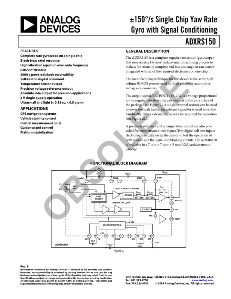
FUNCTIONAL BLOCK DIAGRAM
+ 5V –
100nF
3A
ST1
5G
4G
SELF
TEST
SUMJ
1C
CMID
AGND
2G
1F
AVCC
ST2
COUT
100nF
1D
ROUT
CORIOLIS SIGNAL CHANNEL
RATE
SENSOR
RSEN2
RSEN1
180kΩ 1%
π DEMOD
≈9kΩ ±35% ≈9kΩ ±35%
O
1B
2A
RESONATOR LOOP
1E
2.5V REF
RATEOUT
2.5V
PTAT
3G TEMP
12V
CHARGE PUMP/REG.
PDD
4A
CP2
ADXRS150
5A
22nF
7E
6G
7F
PGND
CP1
6A
7B
CP4
7C
CP3
7D
CP5
47nF
100nF
22nF
Figure 1.
Rev. B
Information furnished by Analog Devices is believed to be accurate and reliable.
However, no responsibility is assumed by Analog Devices for its use, nor for any
infringements of patents or other rights of third parties that may result from its use.
Specifications subject to change without notice. No license is granted by implication
or otherwise under any patent or patent rights of Analog Devices. Trademarks and
registered trademarks are the property of their respective owners.
One Technology Way, P.O. Box 9106, Norwood, MA 02062-9106, U.S.A.
Tel: 781.329.4700
www.analog.com
Fax: 781.326.8703
© 2004 Analog Devices, Inc. All rights reserved.
ADXRS150
TABLE OF CONTENTS
Increasing Measurement Range ............................................... 10
Absolute Maximum Ratings............................................................ 4
Temperature Output and Calibration...................................... 10
Rate Sensitive Axis........................................................................ 4
Using the ADXRS150 with a Supply-Ratiometric ADC ...... 10
ESD Caution.................................................................................. 4
Null Adjustment ......................................................................... 10
Pin Configurations and Function Descriptions ........................... 5
Self-Test Function ...................................................................... 10
Typical Performance Characteristics ............................................. 6
Continuous Self-Test.................................................................. 10
Theory of Operation ........................................................................ 9
Acceleration Sensitivity ............................................................. 11
Supply and Common Considerations ....................................... 9
Outline Dimensions ....................................................................... 12
Setting Bandwidth ........................................................................ 9
Ordering Guide .......................................................................... 12
LE
REVISION HISTORY
TE
Specifications..................................................................................... 3
B
SO
3/04—Data Sheet Changed from Rev. A to Rev. B
Updated Format..................................................................Universal
Changes to Table 1 Conditions ....................................................... 3
Added Evaluation Board to Ordering Guide .............................. 12
O
1/03—Data Sheet Changed from Rev. 0 to Rev. A
Edit to Figure 5.................................................................................. 5
Rev. B | Page 2 of 12
ADXRS150
SPECIFICATIONS
@TA = 25°C, VS = 5 V, bandwidth = 80 Hz (COUT = 0.01 µF), angular rate = 0°/s, ±1g, unless otherwise noted.
Table 1.
O
Min1
±150
11.25
11.25
ADXRS150ABG
Typ
Max1
12.5
13.75
13.75
0.1
0.7
TE
Conditions
Clockwise rotation is positive output
Full-scale range over specifications range
@25°C
VCC = 4.75 V to 5.25 V
Best fit straight line
VCC = 4.75 V to 5.25 V
2.50
@25°C
LE
Delta from 25°C
Power on to ±½°/s of final
Any axis
VCC = 4.75 V to 5.25 V
ST1 pin from Logic 0 to 1, –40°C to +85°C
ST2 pin from Logic 0 to 1, –40°C to +85°C
Standard high logic level definition
Standard low logic level definition
To common
–400
+400
3.3
IOUT = ±100 µA
0.05
°/s/√Hz
40
14
Hz
kHz
–660
+660
–1000
+1000
1.7
2.50
50
8.4
0.25
1000
mV
mV
V
V
kΩ
V
µA
mV/°K
VS – 0.25
V
pF
2.45
2.5
200
5.0
1.0
5.0
2.55
V
µA
mV/mA
mV/V
mV
4.75
5.00
6.0
5.25
8.0
V
mA
+85
°C
Source
0 < IOUT < 200 µA
4.75 VS to 5.25 VS
Delta from 25°C
–40
1
°/s
mV/°/s
mV/°/s
% of FS
%/V
35
0.2
1
50
Source to common
Proportional to absolute temperature
Unit
V
mV
ms
°/s/g
°/s/V
±300
22 nF as comp cap (see the Applications section)
B
SO
Parameter
SENSITIVITY
Dynamic Range2
Initial
Over Temperature3
Nonlinearity
Voltage Sensitivity
NULL
Initial Null
Null Drift over Temperature3
Turn-On Time
Linear Acceleration Effect
Voltage Sensitivity
NOISE PERFORMANCE
Rate Noise Density
FREQUENCY RESPONSE
3 db Bandwidth4 (User Selectable)
Sensor Resonant Frequency
SELF TEST
ST1 RATEOUT Response5
ST2 RATEOUT Response5
Logic 1 Input Voltage
Logic 0 Input Voltage
Input Impedance
TEMPERATURE SENSOR
VOUT at 298°K
Max Current Load on Pin
Scale Factor
OUTPUT DRIVE CAPABILITY
Output Voltage Swing
Capacitive Load Drive
2.5 V REFERENCE
Voltage Value
Load Drive to Ground
Load Regulation
Power Supply Rejection
Temperature Drift3
POWER SUPPLY
Operating Voltage Range
Quiescent Supply Current
TEMPERATURE RANGE
Specified Performance Grade A
All min and max specifications are guaranteed. Typical specifications are not tested or guaranteed.
Dynamic range is the maximum full-scale measurement range possible, including output swing range, initial offset, sensitivity, offset drift, and sensitivity drift at
5 V supplies.
3
Specification refers to the maximum extent of this parameter as a worst-case value at TMIN or TMAX.
4
Frequency at which response is 3 dB down from dc response with specified compensation capacitor value. Internal pole forming resistor is 180 kΩ. See the Setting
Bandwidth section.
5
Self-test response varies with temperature. See the Self-Test Function section for details.
2
Rev. B | Page 3 of 12
ADXRS150
ABSOLUTE MAXIMUM RATINGS
Table 2.
RATE SENSITIVE AXIS
Parameter
Acceleration (Any Axis, Unpowered, 0.5 ms)
Acceleration (Any Axis, Powered, 0.5 ms)
+VS
Output Short-Circuit Duration
(Any Pin to Common)
Operating Temperature Range
Storage Temperature
Rating
2000 g
2000 g
–0.3 V to +6.0 V
This is a Z-axis rate-sensing device that is also called a yaw rate
sensing device. It produces a positive going output voltage for
clockwise rotation about the axis normal to the package top, i.e.,
clockwise when looking down at the package lid.
Indefininte
–55°C to +125°C
–65°C to +150°C
RATEOUT
RATE
AXIS
VCC = 5V
LONGITUDINAL
AXIS
4.75V
2.5V
7
RATE IN
1
TE
A1
ABCDEFG
LATERAL AXIS
Figure 2. RATEOUT Signal Increases with Clockwise Rotation
Applications requiring more than 200 cycles to MIL-STD-883
Method 1010 Condition B (–55°C to +125°C) require underfill
or other means to achieve this requirement.
B
SO
Drops onto hard surfaces can cause shocks of greater than
2000 g and exceed the absolute maximum rating of the device.
Care should be exercised in handling to avoid damage.
ESD CAUTION
O
ESD (electrostatic discharge) sensitive device. Electrostatic charges as high as 4000 V readily accumulate on the
human body and test equipment and can discharge without detection. Although this product features
proprietary ESD protection circuitry, permanent damage may occur on devices subjected to high energy
electrostatic discharges. Therefore, proper ESD precautions are recommended to avoid performance
degradation or loss of functionality.
Rev. B | Page 4 of 12
0.25V
GND
LE
Stresses above those listed under Absolute Maximum Ratings
may cause permanent damage to the device. This is a stress rating only and functional operation of the device at these or any
other conditions above those indicated in the operational section of this specification is not implied. Exposure to absolute
maximum rating conditions for extended periods may affect
device reliability.
ADXRS150
PIN CONFIGURATION AND FUNCTION DESCRIPTIONS
PGND
PDD
CP5
CP3
CP4
7
6
ST1
CP1
5
ST2
CP2
4
AVCC 3
TEMP
TE
2
AGND
G
F
2.5V
CMID
E
D
RATEOUT
SUMJ
C
B
A
Table 3. Pin Function Descriptions
Description
HV Filter Capacitor—47 nF
Charge Pump Capacitor—22 nF
Charge Pump Capacitor—22 nF
Charge Pump Capacitor—22 nF
Charge Pump Capacitor—22 nF
+ Analog Supply
Rate Signal Output
Output Amp Summing Junction
HF Filter Capacitor—100 nF
2.5 V Precision Reference
Analog Supply Return
Temperature Voltage Output
Self-Test for Sensor 2
Self-Test for Sensor 1
Charge Pump Supply Return
+ Charge Pump Supply
B
SO
Mnemonic
CP5
CP4
CP3
CP1
CP2
AVCC
RATEOUT
SUMJ
CMID
2.5V
AGND
TEMP
ST2
ST1
PGND
PDD
O
Pin No.
6D, 7D
6A, 7B
6C, 7C
5A, 5B
4A, 4B
3A, 3B
1B, 2A
1C, 2C
1D, 2D
1E, 2E
1F, 2G
3F, 3G
4F, 4G
5F, 5G
6G, 7F
6E, 7E
LE
Figure 3. BGA-32 (Bottom View)
Rev. B | Page 5 of 12
03226-B-003
1
ADXRS150
TYPICAL PERFORMANCE CHARACTERISTICS
NO PRIOR WARMUP, 0.6Hz SAMPLING
4.5
2.570
4.0
2.565
3.0
2.560
RATEOUT (V)
RATEOUT (V)
3.5
2.5
2.0
1.5
2.555
2.550
1.0
2.545
0
–0.05
0
0.05
0.10
TIME (sec)
0.20
0.15
TE
03226-B-004
0.5
2.540
0.25
0
Figure 4. Rate Sensing Start-Up Time
90
TIME (sec)
120
180
150
Figure 7. Null Settling Time
0.07
LE
2.570
0.06
2.565
0.05
2.560
0.04
°/s
2.555
0.03
2.550
2.545
2.540
0
600
B
SO
RATEOUT (V)
60
30
1200
1800
TIME (sec)
2400
3000
0.02
0.01
0
1
3600
Figure 5. Null Stability for 1 Hour
100
10
TIME (sec)
Figure 8. Root Allan Variance vs. Averaging Time
2.5040
3.4
3.2
O
2.5035
2.5030
2.8
V2.5 (V)
VTEMP (V)
3.0
2.6
2.4
2.5025
2.5020
2.2
2.5015
2.0
2.5010
1.8
–55
–30
–5
45
20
TEMPERATURE (°C)
70
–40 –30 –20 –10
95
Figure 6. Temperature Sensor Output
20 30
0 10
40
TEMPERATURE (°C)
50
60
70
Figure 9. 2.5 V Voltage Reference vs. Temperature
Rev. B | Page 6 of 12
80
ADXRS150
@ BW = 40 Hz, Typical Vibration Characteristics, 10 g Flat Band, 20 Hz to 2 kHz
PACKAGE LATERAL AXIS (0.5s Average)
2.500
2.490
2.490
RATEOUT (V)
RATEOUT (V)
PACKAGE LATERAL AXIS (1/60 SEC SAMPLE RATE)
2.500
2.480
2.470
2.460
2.480
10g
2.470
TE
2.460
2.450
2.450
0
10
5
TIME (sec)
5
TIME (sec)
0
Figure 10. 10 g Random Vibration in Package-Lateral Axis Orientation
PACKAGE LONGITUDINAL AXIS (1/60 SEC SAMPLING RATE)
PACKAGE LONGITUDINAL AXIS (0.5s Average)
LE
2.500
2.490
RATEOUT (V)
2.490
2.480
2.450
0
B
SO
2.470
2.460
5
TIME (sec)
10g
2.480
0g
2.470
2.460
2.450
10
Figure 11. 10 g Random Vibration in Package-Longitudinal Axis Orientation
5
TIME (sec)
0
O
2.490
10
Figure 14. 10 g Random Vibration in Package-Longitudinal Axis Orientation
RATE AXIS (1/60 SEC SAMPLING RATE)
2.500
RATE AXIS (0.5s Average)
2.500
2.490
10g
RATEOUT (V)
RATEOUT (V)
10
Figure 13. 10 g Random Vibration in Package-Lateral Axis Orientation
2.500
RATEOUT (V)
0g
2.480
2.470
2.460
2.480
0g
2.470
2.460
2.450
0
5
TIME (sec)
10
2.450
0
Figure 12. 10 g Random Vibration in Rate Axis Orientation
5
TIME (sec)
10
Figure 15. 10 g Random Vibration in Rate Axis Orientation
Rev. B | Page 7 of 12
ADXRS150
TE
Behavior under Various Shock Test Conditions
Figure 19. Shock Test 100 g, 5 ms in Longitudinal Axis (40 Hz)
B
SO
LE
Figure 16. Shock Test 100 g, 5 ms in Lateral Axis (40 Hz)
Figure 20. Hi-g Shock Test, Lateral Axis, 10× Time Base (40 Hz)
O
Figure 17. Hi-g Shock Test in Lateral Axis (40 Hz)
Figure 18. Hi-g Shock in Rate Axis (40 Hz)
Figure 21. Hi-g Shock, Rate Axis, BW Reduced to 8 Hz
Rev. B | Page 8 of 12
ADXRS150
THEORY OF OPERATION
Only power supplies used for supplying analog circuits are recommended for powering the ADXRS150. High frequency noise
and transients associated with digital circuit supplies may have
adverse effects on device operation.
Figure 22 shows the recommended connections for the
ADXRS150 where both AVCC and PDD have a separate
decoupling capacitor. These should be placed as close to their
respective pins as possible before routing to the system analog
supply. This will minimize the noise injected by the charge
pump that uses the PDD supply.
It is also recommended to place the charge pump capacitors
connected to the CP1–CP4 pins as close to the part as possible.
These capacitors are used to produce the on-chip high voltage
supply switched at the dither frequency at approximately
14 kHz. Care should be taken to ensure that there is no more
than 50 pF of stray capacitance between CP1–CP4 and ground.
Surface-mount chip capacitors are suitable as long as they are
rated for over 15 V.
LE
B
SO
After the demodulation stage, there is a single-pole low-pass
filter consisting of an internal 9 kΩ resistor (RSEN1) and an
external user-supplied capacitor (CMID). A CMID capacitor of
100 nF sets a 400 Hz ± 35% low-pass pole and is used to limit
high frequency artifacts before final amplification. The bandwidth limit capacitor, COUT, sets the pass bandwidth (see Figure 23
and the Setting Bandwidth section).
CP3 CP5
7B
7C
PDD
7D
7E
ST2 4G
SELF
TEST
3G TEMP
CHARGE
PUMP/REG.
7F
5G
5A
4A
PDD
7E
4A 5A
5V
CP2
ST2
3G
TEMP
2G
1B
1C
RATEOUT SUMJ
1D
1E
CMID
2.5V
1F
AGND
100nF
COUT = 22nF
7D
CP4 CP3 CP5
22nF
47nF
22nF
Figure 23. Block Diagram with External Components
SETTING BANDWIDTH
External capacitors CMID and COUT are used in combination
with on-chip resistors to create two low-pass filters to limit the
bandwidth of the ADXRS150’s rate response. The –3 dB
frequency set by ROUT and COUT is
fOUT = 1/ (2 × π × ROUT × COUT )
NOTE THAT INNER ROWS/COLUMNS OF PINS HAVE BEEN OMITTED
FOR CLARITY BUT SHOULD BE CONNECTED IN THE APPLICATION.
Figure 22. Example Application Circuit (Top View)
6A 7B 7C
100nF
100nF
2A
12V
PGND
ADXRS150
3A
AVCC
6G 7F
CP1
ST1
4G
1E 2.5V
PTAT
6G
O
CP2
CMID
1F
1D
1C
ROUT
CORIOLIS
180kΩ 1%
SIGNAL CHANNEL
RSEN1 RSEN2
π
RATE
DEMOD
1B
SENSOR
RATE≈9kΩ ±35%
2A OUT
RESONATOR LOOP
2.5V REF
47nF
CP1
SUMJ
2G
3A
ST1 5G
COUT
100nF
AGND
PGND
6A
22nF
–
5V
100nF
AVCC
100nF
22nF
CP4
+
03226-B-023
The electrostatic resonator requires 14 V to 16 V for operation.
Since only 5 V is typically available in most applications, a
charge pump is included on-chip. If an external 14 V to 16 V
supply is available, the two capacitors on CP1–CP4 can be omitted, and this supply can be connected to CP5 (Pin 7D) with a
100 nF decoupling capacitor in place of the 47 nF.
SUPPLY AND COMMON CONSIDERATIONS
TE
The ADXRS150 operates on the principle of a resonator gyro.
Two polysilicon sensing structures each contain a dither frame,
which is electrostatically driven to resonance. This produces the
necessary velocity element to produce a Coriolis force during
angular rate. At two of the outer extremes of each frame,
orthogonal to the dither motion, movable fingers are placed
between fixed pickoff fingers to form a capacitive pickoff structure that senses Coriolis motion. The resulting signal is fed to a
series of gain and demodulation stages that produce the electrical rate signal output. The dual-sensor design rejects
external g-forces and vibration. Fabricating the sensor with the
signal conditioning electronics preserves signal integrity in
noisy environments.
and can be well controlled since ROUT has been trimmed during
manufacturing to be 180 kΩ ± 1%. Any external resistor applied
between the RATEOUT (1B,2A) and SUMJ (1C,2C) pins results in
ROUT = (180 kΩ× REXT )/ (180 kΩ + REXT )
Rev. B | Page 9 of 12
ADXRS150
The –3 dB frequency is set by RSEN (the parallel combination
of RSEN1 and RSEN2) at about 4.5 kΩ nominal; CMID is less well
controlled since RSEN1 and RSEN2 have been used to trim the rate
sensitivity during manufacturing and have a ±35% tolerance. Its
primary purpose is to limit the high frequency
demodulation artifacts from saturating the final amplifier stage.
Thus, this pole of nominally 400 Hz @ 0.1 µF need not be
precise. Lower frequency is preferable, but its variability usually
requires it to be about 10 times greater (in order to preserve
phase integrity) than the well-controlled output pole. In general,
both –3 dB filter frequencies should be set as low as possible to
reduce the amplitude of these high frequency artifacts as well as
to reduce the overall system noise.
ADXRS150’s 2.5 V output can be converted and used to make
corrections in software for the supply variations.
INCREASING MEASUREMENT RANGE
The resistor value to use is approximately
TE
Null adjustment is possible by injecting a suitable current to
SUMJ (1C, 2C). Adding a suitable resistor to either ground or
the positive supply is a simple way of achieving this. The nominal 2.5 V null is for a symmetrical swing range at RATEOUT
(1B, 2A). However, a nonsymmetric output swing may be suitable in some applications. Note that if a resistor is connected to
the positive supply, supply disturbances may reflect some null
instability. Digital supply noise should be avoided particularly in
this case (see the Supply and Common Considerations section).
RNULL = ( 2.5 × 180 ,000 )/( VNULL0 – VNULL1 )
VNULL0 is the unadjusted zero-rate output, and VNULL1 is the target
null value. If the initial value is below the desired value, the
resistor should terminate on common or ground. If it is above
the desired value, the resistor should terminate on the 5 V supply. Values typically are in the 1 MΩ to 5 MΩ range.
LE
The full-scale measurement range of the ADXRS150 can be
increased by placing an external resistor between the
RATEOUT (1B, 2A) and SUMJ (1C, 2C) pins, which would
parallel the internal ROUT resistor that is factory-trimmed to
180 kΩ. For example, a 330 kΩ external resistor will give
approximately 8.1 mV/°/sec sensitivity and a commensurate
~50% increase in the full-scale range. This is effective for up to a
4× increase in the full-scale range (minimum value of the parallel resistor allowed is 45 kΩ). Beyond this amount of external
sensitivity reduction, the internal circuitry headroom requirements prevent further increase in the linear full-scale output
range. The drawbacks of modifying the full-scale range are the
additional output null drift (as much as 2°/sec over temperature) and the readjustment of the initial null bias (see the Null
Adjustment section).
NULL ADJUSTMENT
B
SO
If an external resistor is used across RATEOUT and SUMJ, the
parallel equivalent value is substituted into the above equation.
Note that the resistor value is an estimate since it assumes VCC =
5.0 V and VSUMJ = 2.5 V.
TEMPERATURE OUTPUT AND CALIBRATION
O
It is common practice to temperature-calibrate gyros to
improve their overall accuracy. The ADXRS150 has a temperature-proportional voltage output that provides input to such a
calibration method. The voltage at TEMP (3F, 3G) is nominally
2.5 V at 27°C and has a PTAT (proportional to absolute temperature) characteristic of 8.4 mV/°C. Note that the TEMP
output circuitry is limited to 50 µA source current.
Using a 3-point calibration technique, it is possible to calibrate
the ADXRS150’s null and sensitivity drift to an overall accuracy
of nearly 300°/hour. An overall accuracy of 70°/hour or better
is possible using more points. Limiting the bandwidth of the
device reduces the flat-band noise during the calibration process,
improving the measurement accuracy at each calibration point.
USING THE ADXRS150 WITH A
SUPPLY-RATIOMETRIC ADC
The ADXRS150’s RATEOUT signal is nonratiometric, i.e., neither the null voltage nor the rate sensitivity is proportional to
the supply. Instead they are nominally constant for dc supply
changes within the 4.75 V to 5.25 V operating range. If the
ADXRS150 is used with a supply-ratiometric ADC, the
SELF-TEST FUNCTION
The ADXRS150 includes a self-test feature that actuates each of
the sensing structures and associated electronics in the same
manner as if subjected to angular rate. It is activated by standard
logic high levels applied to inputs ST1 (5F, 5G), ST2 (4F, 4G), or
both. ST1 causes the voltage at RATEOUT to change about
–0.66 V, and ST2 causes an opposite change of +0.66 V. The selftest response follows the viscosity temperature dependence of
the package atmosphere, approximately 0.25%/°C.
Activating both ST1 and ST2 simultaneously is not damaging.
Since ST1 and ST2 are not necessarily closely matched, actuating both simultaneously may result in an apparent null bias
shift.
CONTINUOUS SELF-TEST
The one-chip integration of the ADXRS150 gives it higher reliability than is obtainable with any other high volume manufacturing method. Also, it is manufactured under a mature BIMOS
process that has field-proven reliability. As an additional failure
detection measure, power-on self-test can be performed. However, some applications may warrant continuous self-test while
sensing rate. Application notes outlining continuous self-test
techniques are also available on the Analog Devices website.
Rev. B | Page 10 of 12
ADXRS150
ACCELERATION SENSITIVITY
2.60
Vibration rectification for frequencies up to 20 kHz is on the
order of 0.00002(°/s)/(m/s2)2, is not significantly dependent on
frequency, and has been verified up to 400 m/s2 rms.
2.54
2.52
2.50
0
2
2.60
2.58
RATEOUT (V)
STATIC 0.8mV rms
2.56
2.54
2.52
SHAKING 2.4mV rms
2.50
0
2
6
4
8
10
TIME (sec)
Figure 26. Random Vibration (Lateral) 10 kHz to 20 kHz
at 0.01 g/√Hz with 60 Hz Sampling and 0.5 sec Averaging
–60
–70
–80
2.56
RATEOUT (V)
RATEOUT (V)
O
2.58
10
Figure 25. Random Vibration (Lateral) 2 Hz to 40 Hz, 3.2 g rms
The output noise of the part falls away in accordance with the
output low-pass filter and does not contain any spikes greater
than 1% of the low frequency noise. A typical noise spectrum is
shown in Figure 27.
2.60
8
TIME (sec)
B
SO
Away from the 14 kHz resonance the effect is not discernible,
except for vibration frequencies within the angular rate pass
band. This can be seen in Figure 10 to Figure 15 for the various
sensor axes. The in-band effect can be seen in Figure 25. This is
the result of the static g-sensitivity. The specimen used for
Figure 25 had a g-sensitivity of 0.15°/s/g and its total in-band
noise degraded from 3 mV rms to 5 mV rms for the specified
vibration. The effect of broadband vibration up to 20 kHz is
shown in Figure 24 and Figure 26.
6
4
LE
Linear vibration spectral density near the 14 kHz sensor resonance translates into output noise. In order to have a significant
effect, the vibration must be within the angular rate bandwidth
(typically ±40 Hz of the resonance), so it takes considerable
high frequency vibration to have any effect.
2.56
TE
There are two effects of concern, shifts in the static null and
induced null noise. Scale factor is not significantly affected until
the acceleration reaches several hundred m/s2.
2.58
RATEOUT (V)
The sign convention used is that lateral acceleration is positive
in the direction from Pin Column A to Pin Column G of the
package. That is, a device has positive sensitivity if its voltage
output increases when the row of Pins 2A–6A are tipped under
the row of Pins 2G–6G in the earth’s gravity.
2.54
–90
–100
–110
2.52
–120
2.50
0
2
6
4
8
10
–130
0
TIME (sec)
Figure 24. Random Vibration (Lateral) 10 kHz to 20 kHz
at 0.01 g/√Hz with 60 Hz Sampling and 0.5 sec Averaging
10
1000
100
FREQUENCY (Hz)
10000
100000
Figure 27. Noise Spectral Density at RATEOUT –BW = 4 Hz
Rev. B | Page 11 of 12
ADXRS150
OUTLINE DIMENSIONS
A1 CORNER
INDEX AREA
7.00 BSC SQ
7
6
5
4
3
2
1
A
BALL A1
INDICATOR
B
C
BOTTOM
VIEW
TOP VIEW
D
E
F
G
4.80 BSC
3.20
2.50
0.44
0.25
3.65 MAX
TE
DETAIL A
DETAIL A
0.15 MAX
COPLANARITY
0.60
SEATING
0.55
PLANE
0.50
BALL DIAMETER
0.80
BSC
ORDERING GUIDE
Temperature Range
–40°C to +85°C
–40°C to +85°C
Package Description
32-Lead BGA
32-Lead BGA
Evaluation Board
O
B
SO
Model
ADXRS150ABG
ADXRS150ABG-Reel
ADXRS150EB
LE
Figure 28. 32-Lead Chip Scale Ball Grid Array [CSPBGA]
(BC-32)
Dimensions shown in millimeters
© 2004 Analog Devices, Inc. All rights reserved. Trademarks and registered trademarks are the property of their respective owners.
C03226–0–3/04(B)
Rev. B | Page 12 of 12
Package Outline
BC-32
BC-32
