Session #20: Homework Solutions
advertisement
Session #20: Homework Solutions
Problem #1
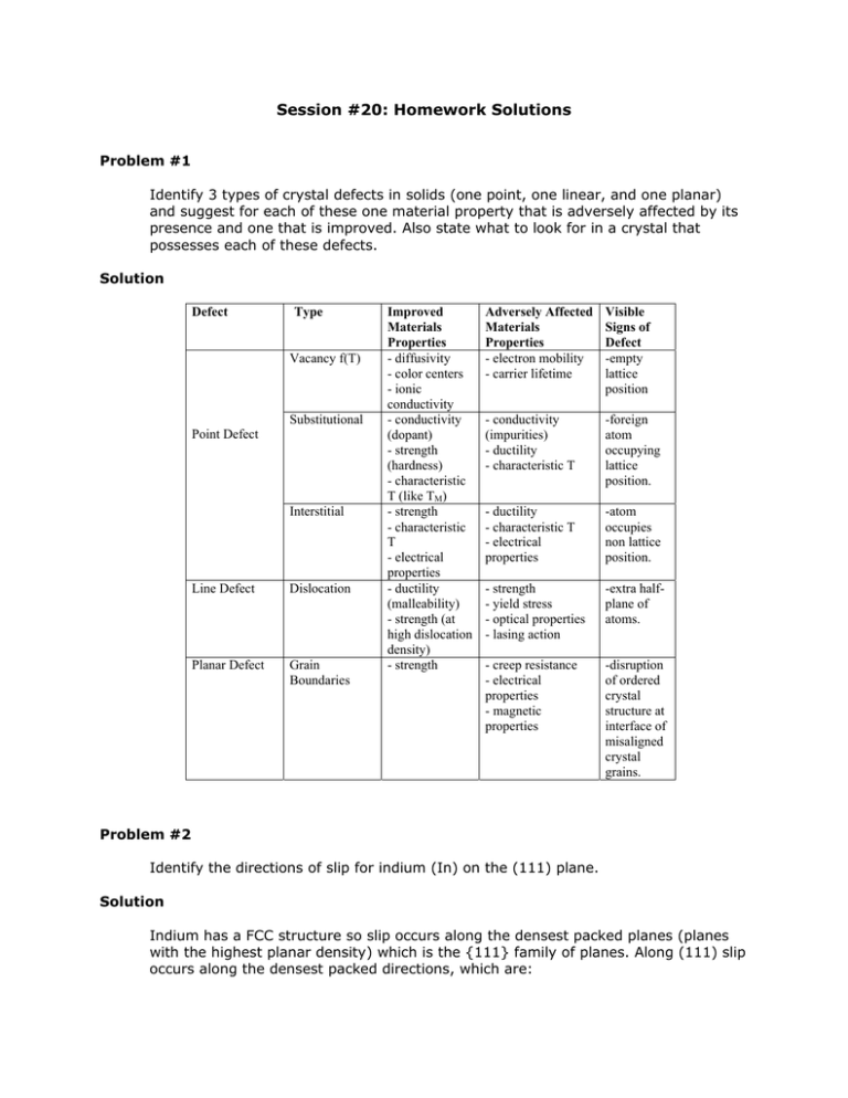
Identify 3 types of crystal defects in solids (one point, one linear, and one planar)
and suggest for each of these one material property that is adversely affected by its
presence and one that is improved. Also state what to look for in a crystal that
possesses each of these defects.
Solution
Defect
Type
Vacancy f(T)
Substitutional
Point Defect
Interstitial
Line Defect
Dislocation
Planar Defect
Grain
Boundaries
Improved
Materials
Properties
- diffusivity
- color centers
- ionic
conductivity
- conductivity
(dopant)
- strength
(hardness)
- characteristic
T (like TM)
- strength
- characteristic
T
- electrical
properties
- ductility
(malleability)
- strength (at
high dislocation
density)
- strength
Adversely Affected
Materials
Properties
- electron mobility
- carrier lifetime
Visible
Signs of
Defect
-empty
lattice
position
- conductivity
(impurities)
- ductility
- characteristic T
-foreign
atom
occupying
lattice
position.
- ductility
- characteristic T
- electrical
properties
-atom
occupies
non lattice
position.
- strength
- yield stress
- optical properties
- lasing action
-extra halfplane of
atoms.
- creep resistance
- electrical
properties
- magnetic
properties
-disruption
of ordered
crystal
structure at
interface of
misaligned
crystal
grains.
Problem #2
Identify the directions of slip for indium (In) on the (111) plane.
Solution
Indium has a FCC structure so slip occurs along the densest packed planes (planes
with the highest planar density) which is the {111} family of planes. Along (111) slip
occurs along the densest packed directions, which are:
⎡110⎤ , ⎡110⎤ , ⎡011⎤ , ⎡011⎤ , ⎡101⎤ , ⎡101⎤
⎣
⎦ ⎣
⎦ ⎣
⎦ ⎣
⎦ ⎣
⎦ ⎣
⎦
Problem #3
A cubic metal (r = 0.77 Å) exhibits plastic deformation by slip along <111>
directions. Determine its planar packing density (atoms/m2) for its densest family of
planes.
Solution
Slip along <111> directions suggests a BCC system, corresponding to {110}, <111>
slip. Therefore:
a 3 = 4r
a=
4r
3
= 1.78 × 10⁻¹⁰ m
Densest planes are {110}, so we find:
2 atoms
a2 2
= 4.46 × 10¹⁹ atoms / m2
Problem #4
(a) List four different defects in crystalline solids.
(b) What evidence is available supporting the actual existence of the listed defects?
Solution
Many answers are acceptable. For example:
(1) dopant elements in semiconductors → affect electrical conductivity
(2) vacancies in close packed metals → explain solid state diffusivity
(3) edge dislocations → explain slip; visible as etch pits and in X–ray topography
(4) grain boundaries → visible in reflected light; evidence by X–ray diffraction
(5) micro–precipitates → visible in X–ray transmission, IR transmission
Problem #5
Attempt to account for the fact that polycrystalline aluminum (Al) has a higher
tensile strength than single crystalline Al. Support your answer with an appropriate
sketch.
Solution
The tensile strength is largely controlled by slip, which in FCC systems such as
aluminum involves the twelve {111} <110> slip systems. The mobility of
dislocations, which controls slip, is high in single crystals because of the high degree
of crystal perfection, so slip proceeds from one external surface to another. In
polycrystalline Al, the mobility of dislocations is slower because of mutual
interference (high density of dislocations) and because precipitates are frequently
encountered, so slip is retarded. Slip, moreover, is arrested at grain boundaries and
deflected in different directions; thus, the strength of polycrystalline material is
higher than that of single crystals.
slip systems in single crystals
slip systems in polycrystalline materials
MIT OpenCourseWare
http://ocw.mit.edu
3.091SC Introduction to Solid State Chemistry
Fall 2009
For information about citing these materials or our Terms of Use, visit: http://ocw.mit.edu/terms.
