Final Review
advertisement
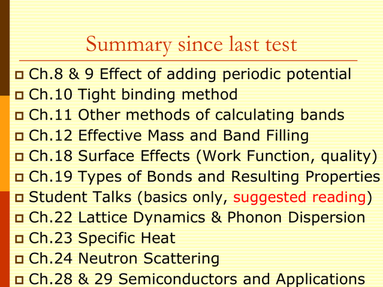
Summary since last test Ch.8 & 9 Effect of adding periodic potential Ch.10 Tight binding method Ch.11 Other methods of calculating bands Ch.12 Effective Mass and Band Filling Ch.18 Surface Effects (Work Function, quality) Ch.19 Types of Bonds and Resulting Properties Student Talks (basics only, suggested reading) Ch.22 Lattice Dynamics & Phonon Dispersion Ch.23 Specific Heat Ch.24 Neutron Scattering Ch.28 & 29 Semiconductors and Applications May need the basics from old stuff, but no direction questions on old stuff FCC Primitive and # of nearest Conventional Unit neighbors Cells Nearest-neighbor distance # of second SC BCC FCC 6 8 12 a ½ a 3 a/2 12 6 6 Review Chapter 8 & 9: Calculate free electron energy bands and the number of k states in the bands Apply Bloch’s theorem to the KronigPenney model or any other periodic potential Explain the meaning and origin of bands and “forbidden band gaps” Understand difference between metals, semiconductors and insulators! Free Electron Brillouin Zone Repeated Zone Scheme 2 2 More generically: h (k 2 / a ) 2 2 (k ) h (k 2n / a ) 2E m nk 2m k –/a 2 /a 2 hk (k ) 2m nk n ,k K nk (r ) n ,k K (r ) Bloch Wavefunctions a Bloch’s Theorem states that for a particle moving in the periodic potential, the wavefunctions ψnk(x) are of the form nk ( x) unk ( x)e , where unk ( x) is a periodic function ikx unk ( x) unk ( x a ) unk(x) has the periodicity of the atomic potential The exact form of u(x) depends on the potential associated with atoms (ions) that form the solid Using Bloch’s Theorem: The Krönig-Penney Model Bloch’s theorem allows us to calculate the energy bands of electrons in a crystal if we know the potential energy function. V V0 -b 0 a a+b x 2a+b 2(a+b) Solve the SE in each region: Energy in terms of E0 Each atom is represented by a finite square well of width a and depth V0. 2K 2 E 2m BAND 2 Forbidden band gap BAND 1 0<x<a I ( x) Ae iKx E0 -b < x < 0 II ( x) Cex De x ka/ iKx Be 2 2 2ma 2 b 2 sin Ka cosKa cos( ka) 2 K Figure 1.7: Coupled Well Energies What happens to these levels as the atoms get closer (b smaller)? How would the energy levels look for multiple wells? Energy Band Overlap Mixing of bands known as hybridization (Si=sp3) Conduction Band The bottom unfilled energy band Valence Band The last filled energy band at T=0 8 14Si: 3s23p2 Out of 8 possible n=3 electrons (2s and 6p) Learning Objectives for Today Chapters 9 - 11: Relate DOS to energy bands Be able to use tight binding model to calculate energy bands Discuss the differences, advantages and disadvantages between various methods of calculating energy bands Predict general features of simple structures LCAO: Electron in Hydrogen Atom (in Ground State) 1 (r) Ae K x1 Second hydrogen atom 2 (r) Ae K x2 2.0 1(r) 1.5 1.0 0.5 0.0 -10 -5 0 5 10 r (aB) Approximation: Only Nearest-Neighbor interactions Group: For 0, 2 and 4 nodes, determine wavefunctions If there are N atoms in the chain c0 there will be N energy levels and N electronic states (molecular orbits). The wavefunction for each electronic state is: c1 c2 c3 c4 k=/a Yk = S eiknacn k=/2a Where: a is the lattice constant, n identifies the individual atoms within the chain, cn represents the atomic orbitals k is a quantum # that identifies the wavefunction and tells us the phase of the orbitals. a k=0 The larger the absolute value of k, the more nodes one has The Independent Electron (e-) Approximation & Sch. Equation 2 2 ( U (r )) k (r ) (k ) k (r ) 2m A SE for each e- is a huge simplification The ind. e- approx. however doesn’t ignore all U(r)=periodic potential + periodic interactions To know U(r), you need To know , you need U(r) Guess U(r), use to solve Use to get better guess of U(r), repeat same The Cellular Method (1934) Since we have periodicity, it is enough to solve the S.E. within a single primitive cell Co The wavefunction in other cell is then k (r R) e k (r ) ik R is a sum over spherical harmonics, need BCs Computationally challenging to solve B.C.s Results in potential with discontinuous derivative at cell boundary Muffin-tin potential Solves both complaints of the last method (set to 0) U(r)=V(|r-R|), when |r-R| ro (the core region) =V(ro)=0, when |r-R| ro (interstitial region) ro is less than half of the nearest neighbor distance Pseudopotential Method Began as an extension of OPW ik r If we act H on e k b c c k (r ) c In the outer region, this gives ~ free energy What goes on in core is largely irrelevant to the energy, so let’s ignore it U(r)=0 , when r Re (the core region) =-e2/r, when r Re (interstitial region) Group: Linear Chain of F F: 1s22s22px22py22pz1 F F F (a) F F F (b) F F (c) F F (d) EF E(k) EF EF 0 k /a 0 k /a 0 EF k /a 0 k Which of the following is the correct band structure for a linear chain of F atoms (atomic #=9)? /a Learning Objectives for Today Chapter 12: Calculate effective mass and cyclotron frequency along certain direcitons Understand the difference between an electron and an electron quasiparticle Distinguish between two types of excitons Two Types of Excitons Wannier – Matt excitons (free exciton): mainly exist in semiconductors, have a large radius, are delocalized states that can move freely throughout the crystal, the binding energy ~ 0.01 eV Frenkel excitons (tight bound excitons): found in insulator and molecular crystals, bound to specific atoms or molecules and have to move by hopping from one atom to another, the binding energy ~ 0.1 -1 eV. Wannier – Matt A phonon is another excitons: quasiparticle stable at cryogenic temperature Frenkel excitons: stable at room temperature Physical Meaning of the Band Effective Mass 2 2 k E * 2m The effective mass is inversely proportional to the curvature of the energy band. Near the bottom of a nearly-free electron band m* is approximately constant, but it increases dramatically near the inflection point and even becomes negative(!) near the zone edge. What does that mean for electron near BZE? Deflection of Electrons in a Uniform Magnetic Field F Bev ma The centripetal acceleration of the electrons is Bev a m v 2 Bev Hence a r m mv r eB which gives Cyclotron frequency Chapter 18 Work function How to measure it and other surface effects Atomic force microscopy Growth mechanisms (e.g., layer by layer) Work function with dipoles Corrections: For finite lattices in 3D, there is a difference compared to infinite lattices F WS Also, non-equivalent crystal faces will have different dipole moments work function depends on the orientation Possibility is that the atoms near surface move Atomic Force Microscope deflection sensor force sensor tip feedback tip sample scanner The force between tip and sample is measured. The interatomic force between tip and sample deflect a cantilever which carries the tip. In this case the vibratio n dampin g Data acquisition Measure roughness to look at quality of film growth. Oriented growth is referred to as epitaxy. Thin film growth is controlled by the interplay of thermodynamics and kinetics. Three growth modes: • Layer-by-layer, or Franck van der Merve growth (typically ideal) • Island, or Vollmer-Weber growth (very rough) • Layer plus island, or Stranski-Krastanov growth (in between) The occurrence of the individual growth modes is governed by the bond strength between the atoms in the layer and the atom-substrate bonds. Chapter 19 Define and compare ionic/covalent bonds Predict properties of materials with different kinds of bonds Guess what kind of bonding should occur for specific materials and back it up with things you’ve learned about bonding Covalent to Ionic Transition Purely Covalen t An ion is an atom in which the total number of electrons is not equal to the total number of protons, giving the atom a net electrical charge. Cation: positive ion Anion: negative ion Purely Ionic Covalent/Ionic Materials Have Strong Bonds Property Melting point and boiling point Electrical conductivity Hardness Explanation Very high melting points because each atom is bound by strong covalent bonds. Many covalent bonds must be broken if the solid is to be melted and a large amount of thermal energy is required for this. Poor conductors because electrons are held either on the atoms or within covalent bonds. They cannot move through the lattice. They are hard because the atoms are strongly bound in the lattice, and are not easily displaced. Brittleness Covalent network substances are brittle. If sufficient force is applied to a crystal, covalent bond are broken as the lattice is distorted. Shattering occurs rather than deformation of a shape. METALLIC PROPERTIES All conduction e-s in a metal combine to form a sea of electrons that move freely between cores high electrical and thermal conductivity. (but weak bond) More electrons=stronger attraction. Means melting and boiling points are higher, and metal is stronger and harder. The free electrons act as the bond (or a “glue”) between the positive ions. This type of bonding is nondirectional and + + + rather insensitive to structure. As a result we have a high ductility of metals: + + + the “bonds” do not “break” when atoms are rearranged – metals can experience a + + + significant degree of plastic deformation. van der Waals Bond From charge fluctuations in atoms due to zero-point motion (due to Heisenberg uncertainty principle); these create attractive dipoles Goes as p2/r6, short ranged Always present, but significant only when other types of bonding not possible Strength of 0.2 eV/atom ~1% of other bonds Because force results from dipole-dipole interactions, it is short range, varying as r -6 graphite Usually with oxygen, fluorine or nitrogen Hydrogen “Bonding” Comes from the fact that it’s really hard (13.6eV) to completely remove an electron from hydrogen • In H20, hydrogen covalently bonds with nearby oxygen, but it also has a hydrogen bond with the next nearest neighbor. • Since the electron is pulled toward the closer oxygen, the positive charge is on the outside and attracted to Chapter 22 Objectives Model simple phonon systems in 1, 2 or 3 dimensions Analyze the dispersion curves for real crystals Explain why neutron scattering is sensitive to the phonon dispersion curve Use to understand experimental specific heat A 2 K K A2 2 2 B cos ka m m K B(eika e ika ) 2 A m K B A(eika e ika ) 2 B M 2 K2 K 2 K 2 2 2 m 2 M 4 Mm cos ka 2 4 2 K B cos ka m K 2 2 m K K B 2 2 2 A cos ka M M •Click on the picture to start the animation M->m note wrong axis inKthe movie 1 1 2 2K m m M 2 K K K K 2 2 2 2 4 4 cos 2 ka Mm M m Mm K K 2 m M 4 A2 2 K M K2 1 cos 2 ka 0 4 Mm 2 2 sin2 ka k : 2a 1 1 1 1 D D m M m M 2 2 2 1 1 1 1 4 sin ka 2 K K Mm m M m M 2 K , m 2 K M 2 Atomic Displacement B m k 0 A M Optic Mode B k 0 1 A Atomic Displacement Click for animations Acoustic Mode Dispersion curves of 3D crystals •3D crystal: clear separation into longitudinal and transverse mode only possible in particular symmetry directions •Every crystal has 3 acoustic branches 1 longitudinal acoustic 2 transverse sound waves of elastic theory •Every additional atom of the primitive basis further 3 optical branches again 2 transverse 1 longitudinal p atoms/primitive unit cell ( primitive basis of p atoms): 3 acoustic branches + 3(p-1) optical branches = 3p branches 1LA +2TA (p-1)LO +2(p-1)TO The energy of other methods Electron X-Ray Neutron λ = 1A° λ = 1A° λ = 2A° E ~ 104 eV E ~ 0.08 eV E ~ 150 eV interact with electron Penetrating interact with nuclei Highly Penetrating interact with electron Less Penetrating SUMMARY: NEUTRON DIFFRACTION Major differences as compared to X-rays – Neutrons are scattered by atomic nuclei – The scattering intensity does not depend on sin, don’t interact with electrons – The energy is ideal for probing phonon dispersion – Scattering by light atoms might be as intense as scattering by heavy atoms – Isotopes of the same element might have different scattering power – Scattering depends on magnetic moments of atoms – Much larger beam and sample are required (due to lower beam intensity). Neutron sources (like high brightness synchrotrons) in the world are limited so neutron diffraction is a very special tool. Treating Phonons like QM Oscillator Einstein Model = Heat capacity C can be found by differentiating the QM average phonon energy Pn n 1 1 n exp n / k T B _ 2 2 n 0 1 exp n / k T B 2 n 0 n 1 n n 2 k BT 1 2 _ 1 2 e / k BT 1 T Einstein Model Fails at Low Temp Einstein model also gave correctly a specific heat tending to zero at absolute zero, but the temperature dependence near T= 0 did not agree with experiment. Why? Taking into account the actual distribution of vibration frequencies in a solid this discrepancy can be accounted for Einstein was aware. He proposed this theory because it was a simple demonstration that QM could solve the specific heat problem. C of Diamond Low Temperature Limit At low T’s, only lattice modes having low frequencies can be excited from their ground states, since the Bose-Einstein function falls to zero for small values of Low frequency sound waves at low T 0 k a Vk 2 dk g 2 2 d k 1 dk 1 vs k vs d vs vs k vs k 2 V 2 vs 1 g 2 2 vs vs depends on the direction V2 1 V2 1 2 g g 3 2 3 2 3 2 vs 2 vL vT Debye approximation has two main steps 1. 2. Approx. of any branch by a linear extrapolation Ensure correct number of modes by imposing a cutoff frequency D , above which there are no modes. Since there are 3N lattice vibration modes in a crystal having N atoms, we choose D so that: D Einstein approximation to the dispersion Debye approximation to the dispersion vk g ( ) g ( )d 3N 0 V 1 2 D 2 ( 3 3 ) d 3N 2 2 vL vT 0 V 1 2 ( 3 3 )D3 3 N 2 6 vL vT V 1 2 3N 9N ( ) 3 2 2 vL3 vT3 D3 D3 9N D3 2 g ( ) / 2 Debye approximation on specific heat at low T 1 2 e 0 / kT g d 1 1 d 2 2 k T Cv V 2 kB 3 3 B dT 15 vL vT 3 The lattice heat capacity of solids varies as T 3at low temperatures; Debye law. Excellent agreement for non-magnetic insulators! Debye motivation: The exact calculation of DOS is hard. Debye obtained a good approximation to the heat capacity by neglecting the dispersion of the acoustic waves, i.e. assuming s k for arbitrary wavenumber. This approximation is still widely used today. Review Chapter 28 & 29: Distinguish between direct and indirect semiconductors and know the difference between their optical absorption Explain photoconductivity Calculate carrier density, chemical potential, and donor binding energies Apply doped semiconductors to explain the pn junction or how to make a transistor 0 or 1 Many solids conduct electricity There are electrons that are not bound but are able to move through the crystal. = n e2 / m ( = 1/) Conducting solids fall into two main classes; metals and semiconductors. ( RT )metals ;106 108 m and increases by the addition of small amounts of impurities (semiconductors do opposite). Impurties have a big effect on semiconductors. Why? Impurities can add states within the band gap that makes excitation (and thus conduction) much more likely (convert) Electron and Hole Densities To determine the number of carriers in each band, we will modify what we derived for free electrons n g ( ) f ( )d Fermi-Dirac distribution function f ( ) and v (E - ) fe (E) exp kB T for c What dependence on energy should the DOS have? Density of States Conduction Band Assume: bottom of conduction band and the top of valence band parabolic conduction band valence band E = Ec + 2k2/2me* E = Ev - 2k2/2mh* 1 Conduction g e (E) = 2 3 2me 2 band Valence band g h (E) = 1 2 2 * 3/2 2m * 3/2 h 3 Ec = Eg ( E Eg ) ( E ) 1 2 1 2 Ev = 0 Valence Band D(E) Conduction Band Valence Band 0 Eg E g (E) V1 2 2 3/ 2 1/ 2 (2 m ) E 3 Electron density in conduction band Density of states Distribution function To find the electron density of occupied states: 1 2me g e (E) = 2 2 2 * 3/2 1 ( E Eg ) 2 (E - ) fe (E) exp kB T Ne g ( E ) f (E)dE e e Eg 3 me * k BT 2 N e 2 exp ( E g ) / k BT ) 2 2 As Ne=Nh(intrinsic) we can say: N e N c N v exp Eg / 2k BT ) This result is important; known as law of mass action; find carrier density without µ. True for both intrinsic & extrinsic semiconductors.
