Lecture 01 Introduction to MEMS
advertisement
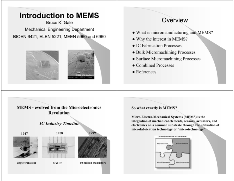
Introduction to MEMS Overview Bruce K. Gale Mechanical Engineering Department BIOEN 6421, ELEN 5221, MEEN 5960 and 6960 MEMS - evolved from the Microelectronics Revolution single transistor 1958 first IC So what exactly is MEMS? Micro-Electro-Mechanical Systems (MEMS) is the integration of mechanical elements, sensors, actuators, and electronics on a common substrate through the utilization of microfabrication technology or “microtechnology”. IC Industry Timeline 1947 What is micromanufacturing and MEMS? ! Why the interest in MEMS? ! IC Fabrication Processes ! Bulk Micromachining Processes ! Surface Micromachining Processes ! Combined Processes ! References ! 1999 10 million transistors MEMS Examples pressure sensors accelerometers flow sensors inkjet printers deformable mirror devices gas sensors micromotors microgears lab-on-a-chip systems MEMS Timeline 1980 1999 Bulk micromachined pressure sensor 2030 TI DMD The Opportunity of MEMS Technology (1.3 million micro-mirrors) ? General MEMS Advantages ! Batch fabrication – Reduced cost ! Reduced size – Is everything better smaller? Reduced power ! High precision ! New capabilities? ! Improved performance? ! Micromachining Processes The MicroTechnology/MEMS Tool Set ! Cleanroom plus microfab processes Standard Integrated Circuit (IC) Processes – Identical to those used in IC fabrication – Generally used for surface micromachining ! + Surface Micromachining – Additive processes ! Bulk Micromachining – Subractive Process ! Dividing line can become very blurry Standard IC Processes Standard IC Processes Photolithography Source: CWRU Source: Jaeger Source: Jaeger Standard IC Processes 1) Deposit/Grow Thin Films • Sputtering • Evaporation • Thermal Oxidation • CVD • Spinning • Epitaxy Standard IC Processes 3) Introduce Dopants (to form electrically-active regions for diodes, transistors, etc.) • Thermal Diffusion • Ion Implantation Standard IC Processes 2) Pattern Thin Films • Lithography • Etching Techniques (wet, dry, RIE) Micromachining Processes Bulk Micromachining • wet vs dry • isotropic vs anisotropic • subtractive process Micromachining Processes Micromachining Processes Bulk Micromachining Deep Reactive Ion Etching (DRIE) Source: Madou • high density ICP plasma • high aspect ratio Si structures • cost: $500K Source: LucasNova Source: Maluf Source: Maluf Source: STS Source: AMMI Source: STS MEMS Examples Micromachining Processes Source: NovaSensor Pressure Sensor (conventional) Wafer-Level Bonding • glass-Si anodic bonding • Si-Si fusion bonding • eutectic bonding • low temp glass bonding Output Voltage (m V) 60 50 40 30 20 10 0 Source: Maluf Source: EV Source: UofL 0 20 40 60 80 Pressure (PSI) 100 120 Micromachining Processes Micromachining Processes Surface Micromachining LIGA (lithographie, galvanoformung, abformtechnik) • additive process • structural & sacrificial layers • uses x-ray lithography (PMMA), electrodeposition and molding to produce very high aspect ratio (>100) microstructures up to 1000 um tall (1986) Source: Sandia Source: Madou MEMS Examples Micro-structures using LIGA Source: Kovacs Micromachining Processes Poor Man’s LIGA • uses optical epoxy negative-resist (SU-8) developed by IBM to produce high aspect ratio micro-structures (1995) UofL Micro-reaction wells: 150 um wide, 120 um tall, 50 um wall thickness Source: UW Source: Maluf MEMS Examples Micromotors MEMS Examples Optical MEMS (MOEMS) Source: MIT and Berkeley MEMS Examples Pressure Sensor (ultra-miniature) Source: NIST, Simon Fraser, UCLA, and MCNC MEMS Examples Lab-on-a-Chip Systems • separation • dilution • mixing and dispensing • analysis Source: NovaSensor Source: Caliper Integration EFFF Fabrication 1 ! Micromachining processes may be integrated ! Both bulk and surface micromachining may be performed on a single substrate ! Micromachined structures may be integrated with ICs ! ! ! Anisotropic etching of input and output ports in 20% KOH at 65 C with Si3N4 mask Deposit and pattern Ti/Au electrodes on front of wafer Thick photosensitive polyimide or SU-8 used to define flow channels EFFF Fabrication 2 Silicon Conta ct Au Detect or Silicon Polyimide Silicon EFFF Fabrication 3 Output Port ! ! ! Remove Si3N4 membrane Deposit and pattern Ti/Au electrode on glass substrate Bond glass substrate to polyimide using biocompatible UV curable adhesive ! Silicon Completed channel looking from the top Ti Glass Silicon Input Port Channel Polyimide Detector Electrode Channel Electrod Glass Au Ti ! Cross section through channel showing electrodes, polyimide and substrates Completed Cross Section Results- Section Fabrication ResultsSystem Assembly Glass substrate with titanium, gold, and platinum electrode Silicon substrate with input/output ports, gold electrodes and patterned SU-8 Above- Complete device with input/output port connections Right- Complete systems with sample and buffer input, µ-EFFF system, and detectors MEMS Examples Fabrication Results ! ! ! Micrograph of detector wire across channel defined by polyimide Wire is 19 µm wide Location of wire eliminates all end effects Micromachined Tips for FEDs and AFMs Detection Wire Output Port Channel Sidewalls Source: Micron (?) Source: IBM MEMS Examples Neural Probes MEMS Examples Neural Interface Chip Source: Stanford Source: Mich (K. Wise) MEMS Examples Micro-Grippers MEMS Examples Micro-Tweezers Source: Berkeley Source: MEMS Precision Instruments MEMS Examples Optical MEMS (MOEMS) MEMS Examples Accelerometers Source: IMC (Sweden), Maluf and TI Sources: Analog Devices, Lucas NovaSensor, and EG&G IC Sensors MEMS Examples Channels, Nozzles, Flow Structures, and Load Cells MEMS References Fundamentals of Microfabrication; Marc J. Madou Micromachined Transducers Sourcebook; G. Kovacs An Introduction to MEMS Engineering; by Nadim Maluf Silicon Micromachining; by Elwenspoek and Jansen Microsensors; by Richard S. Muller, Roger T. Howe, Stephen D. Senturia, R. Smith (Editors) Micromechanics and Mems : Classic and Seminal Papers to 1990; by W. Trimmer (Editor) Source: EG&G IC Sensors MEMS WWW Bookstore: http://mems.isi.edu/bookstore/
