Overview of MEMS and Microsystems
advertisement
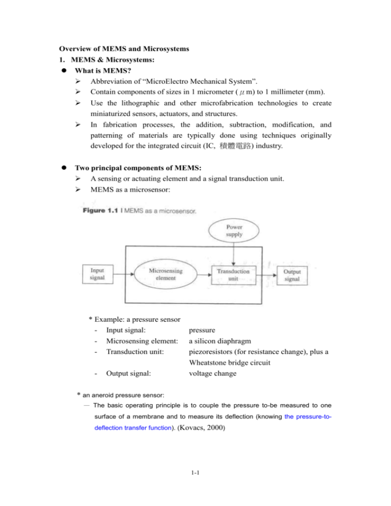
Overview of MEMS and Microsystems 1. MEMS & Microsystems: What is MEMS? Abbreviation of “MicroElectro Mechanical System”. Contain components of sizes in 1 micrometer (μm) to 1 millimeter (mm). Use the lithographic and other microfabrication technologies to create miniaturized sensors, actuators, and structures. In fabrication processes, the addition, subtraction, modification, and patterning of materials are typically done using techniques originally developed for the integrated circuit (IC, 積體電路) industry. Two principal components of MEMS: A sensing or actuating element and a signal transduction unit. MEMS as a microsensor: * Example: a pressure sensor - Input signal: - Microsensing element: - Transduction unit: - Output signal: pressure a silicon diaphragm piezoresistors (for resistance change), plus a Wheatstone bridge circuit voltage change * an aneroid pressure sensor: — The basic operating principle is to couple the pressure to-be measured to one surface of a membrane and to measure its deflection (knowing the pressure-todeflection transfer function). (Kovacs, 1-1 2000) MEMS as a microactuator: * Example: a microgripper Microsystems: 1-2 A microsystem is an engineering system that contains MEMS components that are designed to perform specific engineering functions. 3 components (Madou, 1997): micro sensors, actuators, and a processing unit. Example: an airbag deployment system An intelligent microsystem: Incorporate signal processing and closed-loop feedback control systems into a microsystem. 2. MEMS & Microsystem Products: 2.1 Microgears LIGA toothed wheel (Ruprecht et al., 1997) 1-3 p.s. LIGA: come from the German terms Lithography (Lithographie), electroforming (Galvanoformung), and molding (Abformung). 2.2 Micro mixer Polymer micro mixer (Protron Mikrotechnik) 2.3 Ink-jet Printing Head Principles of Ink-jet Printing: – Drops are shot out from generator G. – – – Drops receive a charge in charging unit C . The electic field E deflects the motion of the drop. The drop lands at the position on the paper. Fig. The essential features of an ink-jet printer. (Halliday et al., 2000)A thermal-bubble-actuated droplet generator (Allen et al., 1-4 1985): An improved droplet generator (Tseng et al., 1998): Comparison of printing results: 1-5 HP 51626A Printhead Microinjector (Tseng, 1998) 2.4 Micro-lens micro-lens (Heckele et al., 1998) 2.5 Micromirrors (微鏡片) 1-6 (a) (b) Fig. Electrostatic Combdrive-Actuated Micromirrors (微鏡片) for Laser-Beam Scanning and Positioning (Kiang et al., 1998) 3. Microfabrication 3.1 Definition The technologies used to produce minute components is called microfabrication technologies, or micromachining. 3.2 Material removal & deposition Removal: The 3-dimensional microstructures can be produced by removing part of the base material by a physical or chemical etching process. Deposition: Thin-film deposition techniques are used to build layers of materials on the base material. 3.3 Evolution The significant amount of microfabrication processes were developed for the microelectronics industry in the past 50 years. - In 1947, transistors (電晶體) were invented. - In 1955, a monolithic (單片的) circuit (i.e., using germanium or silicon to build an entire circuit) was produced at RCA. 1-7 - In 1958, the first IC was produced by Jack Kilby at Texas - Instruments. Today, ultra large scale integration (ULSI) can contain 10 million transistors and capacitors on a chip. 4. Microsystems and Microelectronics 1-8 5. The Multidisciplinary Nature of Microsystem Design and Manufacturing 7 natural science areas are involved: I. Electrochemistry (電化學): ex. electroplating (電鍍; in the LIGA process); fuel cell (燃料電池). II. Electrohydrodynamics III. Molecular biology (分子生物學) IV. Plasma physics (電漿物理) V. Scaling laws VI. Quantum physics (量子物理) VII. Molecular physics (分子物理): molecular dynamics (分子動力學) p.s.: 1. Quantum physics: for example, study the movement of electrons in semiconductor materials. 2. Electrohydrodynamics involves the driving of an ionized fluid by the 1-9 application of electric fields. 5 engineering areas: I. Mechanical engineering II. Electrical engineering III. Chemical engineering IV. Material engineering V. Industrial engineering 6. Microsystems and Miniaturization Benefits of miniaturization: I. Tend to move faster. II. Encounter few problems in thermal distortion and vibration. III. Make them more suitable for applications in medicine and surgery and in microelectronic assemblies. IV. Desirable in satellites and spacecraft engineering. V. Suitable for telecommunication systems. Examples: - Computers: advanced in 50 years from the vacuum-tube technology to the IC technology. → smaller size, but better performance. - Bio-chips: shorter time for disease or virus detection (plus much less samples required). Reference: 1. Halliday, D., Resnick, R., and Walker. J., Fundamentals of Physics: Extended Version 6th ed, Wiley, John & Sons Incorporated, 2000. 2. Hsu, Tai-Ran, MEMS & Microsystems Design and Manufacturing, McGraw-Hill, 2002. 3. Kiang, M.-H., Solgaard, O., Lau, K.Y., and Muller, R.S., 1998, “Electrostatic combdrive-actuated micromirrors for laser-beam scanning and positioning,” Journal of Microelectromechanical Systems, Vol. 7, Issue 1, pp. 27 –37. 4. Kovacs, George T. A., Micromachined Transducers Sourcebook, MaGraw-Hill Companies, Inc., 2000. 1-10
