Department of Electronics and Bio Medical Engineering
advertisement
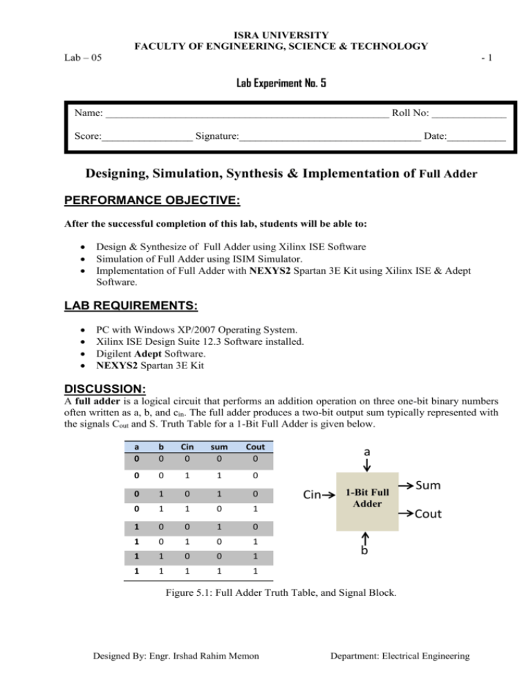
ISRA UNIVERSITY FACULTY OF ENGINEERING, SCIENCE & TECHNOLOGY Lab – 05 -1 Lab Experiment No. 5 Name: _____________________________________________________ Roll No: ______________ Score:_________________ Signature:__________________________________ Date:___________ Designing, Simulation, Synthesis & Implementation of Full Adder PERFORMANCE OBJECTIVE: After the successful completion of this lab, students will be able to: Design & Synthesize of Full Adder using Xilinx ISE Software Simulation of Full Adder using ISIM Simulator. Implementation of Full Adder with NEXYS2 Spartan 3E Kit using Xilinx ISE & Adept Software. LAB REQUIREMENTS: PC with Windows XP/2007 Operating System. Xilinx ISE Design Suite 12.3 Software installed. Digilent Adept Software. NEXYS2 Spartan 3E Kit DISCUSSION: A full adder is a logical circuit that performs an addition operation on three one-bit binary numbers often written as a, b, and cin. The full adder produces a two-bit output sum typically represented with the signals Cout and S. Truth Table for a 1-Bit Full Adder is given below. a 0 b 0 Cin 0 sum 0 Cout 0 0 0 1 1 0 0 1 0 1 0 0 1 1 0 1 1 0 0 1 0 1 0 1 0 1 1 1 0 0 1 1 1 1 1 1 a Cin 1-Bit Full Adder Sum Cout b Figure 5.1: Full Adder Truth Table, and Signal Block. Designed By: Engr. Irshad Rahim Memon Department: Electrical Engineering ISRA UNIVERSITY FACULTY OF ENGINEERING, SCIENCE & TECHNOLOGY Lab – 05 -2 A full adder can be implemented in many different ways such as with a custom transistor-level circuit or composed of other gates. One example implementation is with Figure 5.2: Circuit Diagram of 1-Bit Full Adder DESIGNING PROCEDURE: STEP1: DESIGN ENTRY 1. Invoke Xilinx ISE Design Suite 12.3 Software. “Select File > New Project” 2. Enter the Project name full_adder in the Name field. Verify that HDL is selected as the TopLevel Source Type, and click on NEXT again click on NEXT and Click on Finish. 3. Now Create a New Source file; Go to Project > New Source. Select VHDL Module and Enter the source file name full_adder. Click on Next. Enter the Input and output Ports name and click NEXT and click Finish. VHDL Code for the Full adder is LIBRARY ieee; USE IEEE.STD_LOGIC_1164.ALL ENTITY full_adder is Port (a, b, Cin : in STD_LOGIC; Sum, Cout : in STD_LOGIC; END full_adder; ARCHITECTURE Behavioral of full_adder IS BEGIN sum <= (a XOR b) XOR Cin; Cout <= (a AND b) OR (Cin AND (a XOR b)); END Behavioral; Step 2: Simulation After Creating project and new Source File now it is ready to simulate the Design. To simulate the Full Adder follow the following steps. Designed By: Engr. Irshad Rahim Memon Department: Electrical Engineering ISRA UNIVERSITY FACULTY OF ENGINEERING, SCIENCE & TECHNOLOGY Lab – 05 -3 1. In the Design Panel, select the Simulation radio button. 2. Select full_adder Behavioral file and double click on Simulator Behavioral Model in the Process window. 3. Select the Simulation from the menu bar and click on Restart. 4. Force the input signal (a, b, cin). 5. Select the Simulation from the menu bar and click on Run. It shows the following Simulation result of Full Adder. Figure: 5.3. Simulation Result for Full adder Step 3: Synthesis 1. To synthesize the design, double click on the Synthesize Design option in the Processes window. 2. Now the schematic diagram of the Full adder can be viewed by double clicking View RTL Schematic under Synthesize-XST menu in the Process Window, (Figure5.4). 3. Similarly you can view the Technology Schematic Symbol by double clicking View Technology Schematic under Synthesize-XST menu in the Process Window, (Figure 5.5). Fig: 5.4. Schematic diagram for Full adder Designed By: Engr. Irshad Rahim Memon Fig: 5.5. Technology Schematic Symbol for Full adder Department: Electrical Engineering ISRA UNIVERSITY FACULTY OF ENGINEERING, SCIENCE & TECHNOLOGY Lab – 05 -4 Step 4: Implementation 1. Before implement the design you must create the User Constraint File UCF. 2. After creating the UCF file Single Click on full_adder.ucf file from within Project Navigator, and then Select “Edit Constraints (Text)” from the Process window. 3. Assigning the pins to inputs and outputs of Full adder as following and save Ucf file. NET "a" LOC = "G18"; NET "b" LOC = "H18"; NET "Cin" LOC = "K18"; NET "sum” LOC = "J14"; NET "Cout" LOC = "J15"; 4. After assigning the Pins double click on “Implement Design” option in the Processes window. It will go through steps like Translate, Map and Place & Route. 5. Now create a programming file (bit stream file) of the design. This is done by clicking once on your top-level design in the Sources Pane, followed by a double click on “Generate Programming File” in the process window. 6. Once the programming file (bit stream file) is generated, the file has to be downloaded to the NEXYS2 Spartan3E device, using Digilent Adept Software. Review Question Select NEXYS2 Spartan3E FPGA design the 4-Bit Full adder. Final Assignment : 1. Design Half-bit Adder 2. Simulate “4-Bit Full Adder”; and Attach simulation Result. 3. Designed the 4-Bit Full Adder, perform Synthesis Process, attach the Schematic diagram and Technology Schematic Symbol. Designed By: Engr. Irshad Rahim Memon Department: Electrical Engineering
