Xilinx Tutorial 2
advertisement
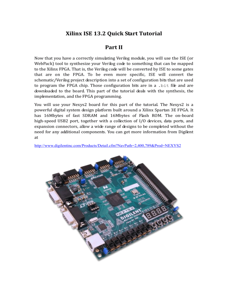
Xilinx ISE 13.2 Quick Start Tutorial Part II Now that you have a correctly simulating Verilog module, you will use the ISE (or WebPack) tool to synthesize your Verilog code to something that can be mapped to the Xilinx FPGA. That is, the Verilog code will be converted by ISE to some gates that are on the FPGA. To be even more specific, ISE will convert the schematic/Verilog project description into a set of configuration bits that are used to program the FPGA chip. Those configuration bits are in a .bit file and are downloaded to the board. This part of the tutorial deals with the synthesis, the implementation, and the FPGA programming. You will use your Nexys2 board for this part of the tutorial. The Nexys2 is a powerful digital system design platform built around a Xilinx Spartan 3E FPGA. It has 16Mbytes of fast SDRAM and 16Mbytes of Flash ROM. The on-board high-speed USB2 port, together with a collection of I/O devices, data ports, and expansion connectors, allow a wide range of designs to be completed without the need for any additional components. You can get more information from Digilent at http://www.digilentinc.com/Products/Detail.cfm?NavPath=2,400,789&Prod=NEXYS2 Realizing a circuit design on an FPGA board consists of three steps, which are performed using a software tool like Xilinx ISE, a tool from Xilinx which integrates various stages of the FPGA design cycle into one software tool: 1) Synthesis: This is the process of converting a Verilog description into a primitive gate-level netlist. The final product of the design partitioning phase is a netlist file, a text file that contains a list of all the instances of primitive components in the translated circuit and a description of how they are connected. 2) Implementation: a. Translation: The translate step takes all of the netlists and design constraints information and outputs a Xilinx NGD (native generic database) file. b. Mapping: The mapping step maps the above NGD file to the technology-specific components on the FPGA and generates an NCD (native circuit description) file. This is necessary because different FPGAs have different architectures, resources, and components. Among other tasks, it is responsible for the process of transforming the primitive gates and flip-flops in the netlist into LUTs (lookup tables) and other primitive FPGA elements. For example, if you described a circuit composed of many gates, but ultimately of 6 inputs and 1 output, the circuit will be mapped down to a single 6-LUT. Likewise, if you described a flip-flop it will be mapped to a specific type of flip-flop that actually exists on the FPGA. c. Placement: This step places the mapped components in a manner that minimizes wiring, delay etc. Placement takes a mapped design and determines the specific location of each component in the design on the FPGA. d. Routing: This step configures the programmable interconnects (wires) so as to wire the components in the design. Because the number of possible paths for a given signal is very large, and there are many signals, this is typically the most time-consuming part. 3) Programming the FPGA Device: In this step, the placed and routed design is converted to a bit-stream using the Xilinx ISE tool. The bit-stream generated by the tool (as a .bit file) is loaded on to the FPGA. This bit-stream file programs the logic and interconnects of the FPGA in such a way that the design gets implemented. The following figure illustrates the design flow described above. Part 3: User Constraints File Before implementing a circuit on the Nexys2 board, you must associate signal names in your design with physical pin connections and circuits on the board. This is required because I/O devices on the board (like buttons, switches, and LEDs) are physically tied to certain pins on the FPGA device, and the CAD tools must be told which pins are connected to which devices. In our example, we need to tell ISE which pins on the Xilinx chip we want A, B, Cin to be assigned to so that we can access those from switches, and where we want Cout and Sum so we can see those on the LEDs on the Nexys2 board. The Xilinx tools use a “User Constraints File” (.ucf file) to map circuit node names in source files to physical pins on the board. (If no .ucf file is present in a project folder, the Xilinx tools will randomly assign I/O port nodes to physical pins.) The .ucf file should contain entries that specify signal names from your source files and assign those signals to specific pin numbers. Pin numbers for all I/O devices and connectors attached to the FPGA can be found in the Nexys2 board’s reference manual and/or schematic. There are two ways to specify a .ucf file in Xilinx ISE: (i) Create a .ucf module manually using any editor and provide the filename to Xilinx ISE, or (ii) Create a .ucf module in ISE by running the User Constraints processes. For large designs, the second option is better, and so it is described below. 1. Back in the Design pane, return to the Implementation view and select your fulladder schematic. Now in the Processes pane you will see some options including User Constraints, Synthesize, and Implement Design. The first thing you will do is assign pins using the User Constraints tab. Expand that tab and select the I/O Pin Planning (PlanAhead) – Pre-Synthesis choice. This will let you assign signals to pins on the FPGA using the PlanAhead tool. This will open a new tool called PlanAhead which you can use to set your pin constraints. You may have to agree to add a UCF (Universal Constraints File) file to your project. You should agree to this (“Yes”). 2. The PlanAhead tool lets you set a number of different types of constraints on how the circuit is mapped to the Xilinx part. For now we will just use the pin constraints in the UCF file. You can see a list of the I/O ports from your schematic in the RTL pane (click on the I/O Ports tab in the upper left window). You can set which FPGA pin they are attached to using the Site field. 3. Expand Scalar ports and double click on the Site field of each I/O Port in turn. This will allow you to update the Site field to say which FPGA pin should be used for that I/O signal. (Or, you can click one port and edit the Site in the I/O Port Property tab). 4. How do you know which pins to assign the signals to in order to use the switches and LEDs on the Nexys2 board? You can look in the Nexys2 reference manual available from Digilent: http://www.digilentinc.com/Data/Products/NEXYS2/Nexys2_rm.pdf For now, note that the SW3, SW2, SW1 sliding switches on the Nexys2 board, from left to right as you look at the board with the LCD at the bottom, are on pins K17, K18, H18. Here is the diagram from the reference manual: You can find more detailed information from the UCF provided by Digilent: http://www.digilentinc.com/Data/Products/NEXYS2/Nexys2_500General.zip This tells you how to fill out the information in PlanAhead for the switches. Let us put A, B, and Cin on SW3, SW2, and SW1; and use LD1 and LD2 as Sum and Cout. 5. Now save the PlanAhead settings (Save Design button on the top left of the window). This will update things in your main ISE project. 6. When you exit, you will see that a fulladder.ucf file has been added to the project Part 4: Synthesis and Implementation 1. Synthesize – XST. Double click on this to synthesize your circuit. After a while you will (hopefully) get the Process “Synthesize” completed successfully message in the console. If you have already simulated your circuit and verified its correctness, there is every chance that it will synthesize correctly without problems. In any case, there is a lot of interesting information worth looking at in the synthesis report (the data in the console window). Make sure that you end the process with a green check for this process. If you get something else, especially a red X, you will need to fix errors and re-synthesize. 2. With your source file selected (fulladder in this case), double click the Implement Design process in the Processes tab. This will translate the design to something that can physically be mapped to the specific FPGA that is on the Nexys2 board (the xc3s500e-5fg320). You should see a green check mark if this step finishes without issues. If there are issues, you need to read them for clues about what went wrong and what you should look at to fix things. 3. If you expand the Implement Design tab (which is not necessary) you will see that the Implement Design process actually consists of three parts: a. Translate: Translate is the first step in the implementation process. The Translate process merges all of the input netlists and design constraint information, and outputs a Xilinx NGD (Native Generic Database) file. The output NGD file can then be mapped to the targeted FPGA device. b. Map: Mapping is the process of assigning a design’s logic elements to the specific physical elements that actually implement logic functions in a device. The Map process creates an NCD (Native Circuit Description) file. The NCD file will be used by the PAR process. c. Place and Route (PAR): PAR uses the NCD file created by the Map process to place and route your design. PAR outputs an NCD file that is used by the bitstream generator (BitGen) to create a (.bit) file. The Bit file (see the next step) is what is used to actually program the FPGA. 4. At this point you can look at the Design Summary to find out all sorts of things about your circuit. One thing that you might want to do is to click on the Pinout Report and check that your signals were correctly assigned to the pins you wanted them to be assigned to. 5. Now right click Generate Programming File. Then, click Process Properties. From the Startup Options category, set the value of FPGA Start-Up Clock as JTAG Clock. Click OK. Double click Generate Programming File. This will generate the actual configuration bits and write into a .bit file that you can use to program your Nexys2 board so as to behave like your circuit (in this case a full adder). The .bit file is located in the project’s folder. In this example, the location is: C:\ECE\Xilinx\example\example\fulladder.bit Part 4: Program the FPGA To program the Spartan3E on the Nexys2 board we will use the ExPort tool that is part of the Adept Suite available from Digilent at http://www.digilentinc.com/Software/Adept.cfm?Nav1=Software&Nav2=Adept 1. First attach the USB cable to the board WITHOUT launching the Adept software. The USB cable is both the data cable and the power supplier to the Nexys2 board. Make sure the Power Select Jumper is working in the USB mode and power of the board is “On”. 2. Start the Adept software, and wait for the FPGA and the Platform Flash ROM to be recognized. Use the browse function to associate the desired .bit file with the FPGA, and/or the desired .mcs file with the Platform Flash ROM. For our lab, select JTAG mode using the Mode Jumper on the board (keep it connected to the left two pins). 3. Browse the bit file located in the project folder; then, click Program. The configuration file will be sent to the FPGA, and the software will indicate whether programming was successful. Now, you can check the functionalities of a full adder on the board. Overview of the Procedure 1. Design the circuit that you like to map to the FPGA part on the Nexys2 board. You can use schematics, or Verilog, or a mixture of both. 2. Simulate your circuit using the ISE Simulator and a Verilog testbench to provide inputs to the circuit. Use “if” statements in your testbench to make it self-checking. 3. Generate a UCF file to hold constraints such as pin assignments (later we will use the UCF file for other constraints like timing and speed). Use the PlanAhead tool to generate this file. 4. Assign the I/O pins in your design to the pins on the FPGA that you want them connected to. 5. Synthesize the design using the XST synthesis tool. 6. Implement the design to map it to the specific FPGA on the Nexys2 board. 7. Generate the programming file (.bit file) that has the bitstream that will configure the FPGA. 8. Connect your Nexys2 board to the host computer and use the Adept tool to program the FPGA using the bitstream.

