19-4156; Rev 0; 5/08
EVALUATION KIT AVAILABLE
MAX3674 Evaluation Kit
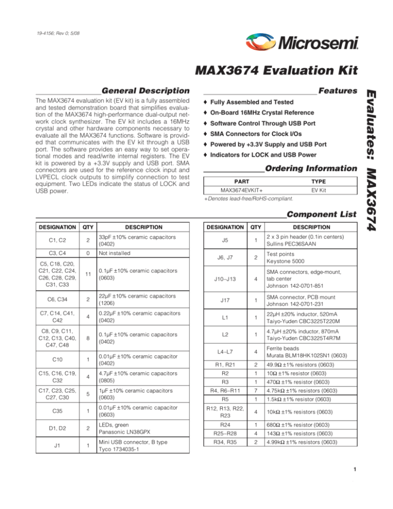
The MAX3674 evaluation kit (EV kit) is a fully assembled
and tested demonstration board that simplifies evaluation of the MAX3674 high-performance dual-output network clock synthesizer. The EV kit includes a 16MHz
crystal and other hardware components necessary to
evaluate all the MAX3674 functions. Software is provided that communicates with the EV kit through a USB
port. The software provides an easy way to set operational modes and read/write internal registers. The EV
kit is powered by a +3.3V supply and USB port. SMA
connectors are used for the reference clock input and
LVPECL clock outputs to simplify connection to test
equipment. Two LEDs indicate the status of LOCK and
USB power.
Features
♦ Fully Assembled and Tested
♦ On-Board 16MHz Crystal Reference
♦ Software Control Through USB Port
♦ SMA Connectors for Clock I/Os
♦ Powered by +3.3V Supply and USB Port
♦ Indicators for LOCK and USB Power
Ordering Information
PART
TYPE
MAX3674EVKIT+
EV Kit
+Denotes lead-free/RoHS-compliant.
Component List
DESIGNATION
QTY
DESCRIPTION
C1, C2
2
33pF ±10% ceramic capacitors
(0402)
C3, C4
0
Not installed
C5, C18, C20,
C21, C22, C24,
C26, C28, C29,
C31, C33
11
C6, C34
DESIGNATION
QTY
DESCRIPTION
J5
1
2 x 3 pin header (0.1in centers)
Sullins PEC36SAAN
J6, J7
2
Test points
Keystone 5000
0.1μF ±10% ceramic capacitors
(0603)
J10–J13
4
SMA connectors, edge-mount,
tab center
Johnson 142-0701-851
2
22μF ±10% ceramic capacitors
(1206)
J17
1
SMA connector, PCB mount
Johnson 142-0701-231
C7, C14, C41,
C42
4
0.22μF ±10% ceramic capacitors
(0402)
L1
1
22μH ±20% inductor, 520mA
Taiyo-Yuden CBC3225T220M
C8, C9, C11,
C12, C13, C40,
C47, C48
8
0.1μF ±10% ceramic capacitors
(0402)
L2
1
4.7μH ±20% inductor, 870mA
Taiyo-Yuden CBC3225T4R7M
L4–L7
4
1
0.01μF ±10% ceramic capacitor
(0402)
Ferrite beads
Murata BLM18HK102SN1 (0603)
R1, R21
2
49.9 ±1% resistors (0603)
R2
1
10 ±1% resistor (0603)
R3
1
470 ±1% resistor (0603)
R4, R6–R11
7
4.75k ±1% resistors (0603)
R5
1
1.5k ±1% resistor (0603)
R12, R13, R22,
R23
4
10k ±1% resistors (0603)
C10
C15, C16, C19,
C32
4
4.7μF ±10% ceramic capacitors
(0805)
5
1μF ±10% ceramic capacitors
(0603)
C35
1
0.01μF ±10% ceramic capacitor
(0603)
D1, D2
2
LEDs, green
Panasonic LN38GPX
C17, C23, C25,
C27, C30
J1
1
Mini USB connector, B type
Tyco 1734035-1
R24
1
680 ±1% resistor (0603)
R25–R28
4
143 ±1% resistors (0603)
R34, R35
2
4.99k ±1% resistors (0603)
________________________________________________________________ Maxim Integrated Products
For pricing, delivery, and ordering information, please contact Maxim Direct at 1-888-629-4642,
or visit Maxim’s website at www.maxim-ic.com.
1
Evaluates: MAX3674
General Description
Evaluates: MAX3674
MAX3674 Evaluation Kit
Component List (continued)
DESIGNATION
TP1–TP7, TP10
U1
QTY
DESCRIPTION
8
Test points
Keystone 5000
1
High-performance dual-output
network clock synthesizer
(48 LQFP)
Microsemi
MAX3674ECM+
Maxim
MAX3674ECM+
DESIGNATION
QTY
DESCRIPTION
U5
1
Buffer (5 SC-70)
Fairchild NC7SV125P5X
Y1
1
16.000MHz SMD crystal, 18pF
Citizen HCM49-16.000MABJ-UT
Y2
1
6.000MHz SMD crystal, 32pF
ECS ECS-60-32-5PXDN-TR
U2
1
Microcontroller (28 SO)
Microchip PIC16C745-I/SO
None
2
Shunts for J5
Sullins SSC02SYAN
U3
1
Dual level translator (8 SOT23)
Maxim MAX3373EEKA+
None
1
PCB: MAX3674 EV Kit+ Circuit
Board, Rev A
U4
1
I/O port expander (24 TQFN)
Maxim MAX7312ATG+
Quick Start
Note: In the following sections, software-related items
are identified by bolding. Text in bold refers to items
directly from the EV kit software. Text in bold and
underlined refers to items from the Windows® operating
system.
1) Install two shunts on jumper J5, both to the (L) position. This sets address pins ADR0 and ADR1 low.
2) Connect a +3.3V supply to VCC (J6) and GND (J7).
Set the supply current limit to 200mA.
3) Connect the computer to the EV kit with a USB
cable (A-Male to Mini-B-Male). LED D2 should
switch on, indicating that USB power is detected.
4) To
To download
downloadthe
thelatest
latestversion
versionof
of the
the EV
EV kit software
(MAX3674revX.zip),
visitatthewww.microsemi.com.
Maxim website at
the
Microsemi website
www.maxim-ic.com/evkitsoftware.
Uncompress
the zip file to a local folderUncompress
and run the
the zip file to
folder and
run the installation
installation
filea local
(setup.exe).
Installation
requires
file (setup.exe).
Installation
requires
administrative
administrative
rights
and may
also require
Internet
rights to
and
may also
requiredrivers.
Internet access to
access
download
necessary
download necessary drivers.
5) After installation is complete, follow this path to start
the program: Start → All Programs → Maxim
Integrated Products → MAX3674 Evaluation Kit
6) Press the Initialize / Test Communication button.
The message box should report:
USB Device Detected
MAX3674 Detected
MAX7312 Detected
7) Press the following buttons in this order: RESET →
LOAD → READ. At this point, the LOCK output
should be high (LED D1 on), indicating that the PLL
is locked.
8) Set the values for P, NA, NB, and M to obtain the
desired output frequency.
9) Press the LOAD button, followed by the READ button.
10) Connect the clock outputs (QA, QA, QB, QB) to test
equipment with SMA cables. Terminate unused outputs.
Windows is a registered trademark of Microsoft Corp.
2
_______________________________________________________________________________________
MAX3674 Evaluation Kit
The MAX3674 EV kit simplifies evaluation by providing
the hardware and software needed to evaluate all the
MAX3674 functions. A microcontroller (Microchip
PIC16C745) and I/O port expander (MAX7312) allow
the user to set control pins and read/write registers with
software. The on-board 16MHz crystal and integrated
oscillator generate the PLL reference clock.
Alternatively, an external clock source can be connected to the REF_CLK input to serve as the reference
clock. LED D1 switches on when the LOCK output is
high, indicating the PLL is locked.
The microcontroller is powered by the USB port +5V
supply. LED D2 switches on when USB power is
detected. The MAX3674 and I/O port expander are
powered by the +3.3V supply. The EV kit also includes
the MAX3373 level translator that interfaces the I2C
clock and data lines from the microcontroller to the
MAX3674 and I/O port expander, and is powered by
both supplies. The USB cable and +3.3V supply can
be connected to the EV kit in any sequence.
Master Reset
It is recommended to press the RESET button after
every power-up.
LVPECL Clock Outputs
The LVPECL clock outputs (QA, QA, QB, QB) have onboard bias-Ts that provide DC biasing and AC-couple
the signal to allow direct connection to 50Ω-terminated
test equipment. Unused outputs should be terminated
to prevent reflections on the transmission lines.
Reference Clock Input
The REF_CLK input (J17) accepts sinusoidal or squarewave clocks with frequencies between 15MHz and
20MHz, and swings up to 3.3VP-P. This input has a 50Ω
DC termination to ground and is AC-coupled to an onboard buffer. The buffer is used to square the clock
signal applied to the REF_CLK input pin.
I2C Slave Address
Jumper J5 is used to set the two selectable address
bits (ADR0 and ADR1). The EV kit software performs a
search at power-up to determine which of the four possible slave addresses is being used.
EV Kit Software
The EV kit software provides an easy way to set operational modes and read/write internal registers
(Figure 1). Refer to the MAX3674 data sheet for
detailed descriptions of the MAX3674 functions and
guidance on selecting dividers settings. Note that when
the Programming Interface is set to I2C, the settings
for dividers P, NA, NB, and M are configured within the
MAX3674 after pressing the LOAD button.
_______________________________________________________________________________________
3
Evaluates: MAX3674
Detailed Description
Evaluates: MAX3674
MAX3674 Evaluation Kit
Figure 1. MAX3674 EV Kit Software
4
_______________________________________________________________________________________
_______________________________________________________________________________________
C30
1μF
C2
33pF
1
2
6
5
4
3
2
1
C31
0.1μF
C1
33pF
Y2
6.0MHz
I/O5
I/O4
I/O3
I/O2
I/O1
I/O0
C22
0.1μF
14
13
12
11
10
9
8
7
6
5
4
3
2
1
VCC
U4
MAX7312
D-
D+
RC6
RC7
VSS
VDD
RB0
RB1
RB2
RB3
RB4
RB5
RB6
RB7
R5
1.5kΩ
U2
PIC16C745
C21
0.1μF
VUSB
RC2
RC1
RC0
OSC2
OSC1
VSS
RA5
RA4
RA3
RA2
RA1
RA0
MCLR
I/O11
I/O12
I/O13
I/O14
I/O15
AD0
15
16
17
18
19
20
21
22
23
24
25
26
27
28
13
14
15
16
17
18
C19
4.7μF
R7
4.75kΩ
LED
D2
C20
0.1μF
1
R8
4.75kΩ
R9
4.75kΩ
TP2
CLK_STOPB
R35
4.99kΩ
VCC
C18
0.1μF
R10
4.75kΩ
R34
C5
0.1μF 4.99kΩ
C17
1μF
R24
680Ω
TP4
CLK_STOPA
R1
49.9Ω
J17
C15
4.7μF
L1
22μH
USB_PWR
2
SMAPCB
REF_CLK
C16
4.7μF
VUSB TP6
VUSB
R6
4.75kΩ
3
2
1
GND
NC
D+
D-
VBUS
VCC
GND
A
OE
Y
VCC
4
5
J1
MINI-B USB
R12
10kΩ
U5
NC7SV125P5X
5
4
3
2
1
R11
4.75kΩ
C6
22μF
C48
0.1μF
VCC
R2
10Ω
R13
10kΩ
C25
1μF
C4
OPEN
C10
0.01μF
R22
10kΩ
C26
0.1μF
C3
OPEN
9
8
7
6
5
4
3
2
1
5
VCC
12
11
C40
0.1μF
C9
0.1μF
1
3
10
VCC
VCC
C29
0.1μF
C8
0.1μF
Y1
16.0MHz
1
2
R23
10kΩ
VCC
SCL
SDA
J5
XTAL2
XTAL1
CLK_STOPB
CLK_STOPA
GND
REF_CLK
SCL
SDA
I/O VL2
VL
GND
I/O VCC2
VCC
REF_SEL
VCC_PLL
VCC
GND
BYPASS
VCC
6
4
2
4
3
2
1
VCC
I/O VCC1
VCC
I/O VL1
THREE-STATE
MAX3373
U3
43
20
C24
0.1μF
U1
MAX3674
41
C23
1μF
5
6
7
8
VCC VUSB
38
VUSB
46
R4
4.75kΩ
VCC
24
C27
1μF
37
TEST_EN
LOCK
GND
QB
QB
VCC
GND
QA
QA
VCC
NB
VCC
GND
VUSB
23
AD2
I/O6
7
AD1
22
GND
9
I/O7
8
INT
21
V+
I/O8
10
19
SCL
SDA
I/O9
11
48
P
VCC
13
I/O10
12
47
ADR0
M0
14
45
ADR1
15
M1
44
SCL
M2
16
SDA
17
MR
M4
18
M3
42
VCC
GND
19
40
PLOAD
20
M5
39
NA0
M6
21
NA1
M7
22
NA2
M8
23
M9
24
25
26
27
28
29
30
31
32
33
34
35
36
TP3
TP5
LED
D1
1
2
LOCK
R3
470Ω
LOCK
TP7
C35
0.01μF
VCC C47
0.1μF
C13
0.1μF
C12
0.1μF
C11
0.1μF
VCC
C28
0.1μF
VCC
TP10
R27
143Ω
L7
FERRITE BEAD
L5
FERRITE BEAD
R25
143Ω
TP1
C33
0.1μF
C32
4.7μF
R28
143Ω
L6
FERRITE BEAD
C42
0.22μF
C41
0.22μF
C14
0.22μF
J13
J12
J11
L4
FERRITE BEAD
C7
0.22μF J10
R26
143Ω
L2
4.7μH
SMA
QB
SMA
QB
SMA
QA
SMA
QA
C34
22μF
J7
J6
GND
VCC
Evaluates: MAX3674
VCC
MAX3674 Evaluation Kit
Figure 2. MAX3674 EV Kit Schematic
5
Evaluates: MAX3674
MAX3674 Evaluation Kit
Figure 3. MAX3674 EV Kit Component Placement Guide—Component Side
6
_______________________________________________________________________________________
MAX3674 Evaluation Kit
Evaluates: MAX3674
Figure 4. MAX3674 EV Kit PCB Layout—Component Side
_______________________________________________________________________________________
7
Evaluates: MAX3674
MAX3674 Evaluation Kit
Figure 5. MAX3674 EV Kit PCB Layout—Ground Plane
8
_______________________________________________________________________________________
MAX3674 Evaluation Kit
Evaluates: MAX3674
Figure 6. MAX3674 EV Kit PCB Layout—Power Plane
_______________________________________________________________________________________
9
Evaluates: MAX3674
MAX3674 Evaluation Kit
Figure 7. MAX3674 EV Kit PCB Layout—Solder Side
10
_____________________________________________________________________________________
Microsemi Corporation (NASDAQ: MSCC) offers a comprehensive portfolio of semiconductor
solutions for: aerospace, defense and security; enterprise and communications; and industrial
and alternative energy markets. Products include high-performance, high-reliability analog and
RF devices, mixed signal and RF integrated circuits, customizable SoCs, FPGAs, and
complete subsystems. Microsemi is headquartered in Aliso Viejo, Calif. Learn more at
www.microsemi.com.
Microsemi Corporate Headquarters
One Enterprise, Aliso Viejo CA 92656 USA
Within the USA: +1 (949) 380-6100
Sales: +1 (949) 380-6136
Fax: +1 (949) 215-4996
© 2012 Microsemi Corporation. All rights reserved. Microsemi and the Microsemi logo are trademarks of
Microsemi Corporation. All other trademarks and service marks are the property of their respective owners.


