Design of an Integrated CMOS Integer PLL
advertisement
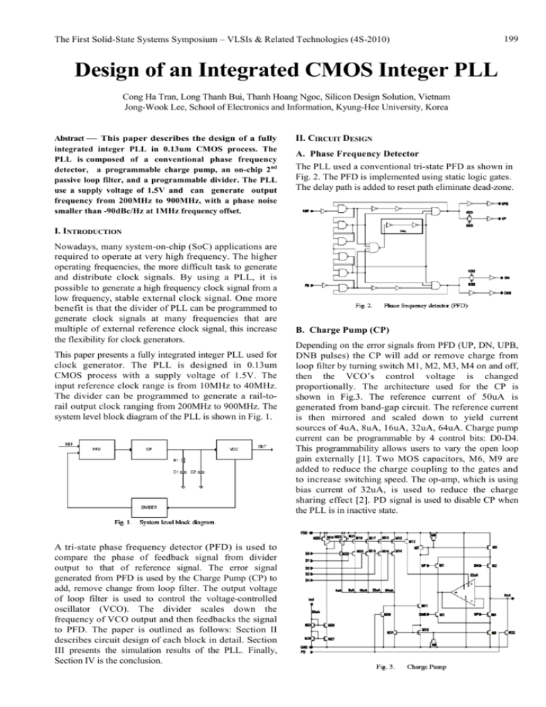
The First Solid-State Systems Symposium – VLSIs & Related Technologies (4S-2010) 199 Design of an Integrated CMOS Integer PLL Cong Ha Tran, Long Thanh Bui, Thanh Hoang Ngoc, Silicon Design Solution, Vietnam Jong-Wook Lee, School of Electronics and Information, Kyung-Hee University, Korea Abstract — This paper describes the design of a fully integrated integer PLL in 0.13um CMOS process. The PLL is composed of a conventional phase frequency detector, a programmable charge pump, an on-chip 2nd passive loop filter, and a programmable divider. The PLL use a supply voltage of 1.5V and can generate output frequency from 200MHz to 900MHz, with a phase noise smaller than -90dBc/Hz at 1MHz frequency offset. II. CIRCUIT DESIGN A. Phase Frequency Detector The PLL used a conventional tri-state PFD as shown in Fig. 2. The PFD is implemented using static logic gates. The delay path is added to reset path eliminate dead-zone. I. INTRODUCTION Nowadays, many system-on-chip (SoC) applications are required to operate at very high frequency. The higher operating frequencies, the more difficult task to generate and distribute clock signals. By using a PLL, it is possible to generate a high frequency clock signal from a low frequency, stable external clock signal. One more benefit is that the divider of PLL can be programmed to generate clock signals at many frequencies that are multiple of external reference clock signal, this increase the flexibility for clock generators. This paper presents a fully integrated integer PLL used for clock generator. The PLL is designed in 0.13um CMOS process with a supply voltage of 1.5V. The input reference clock range is from 10MHz to 40MHz. The divider can be programmed to generate a rail-torail output clock ranging from 200MHz to 900MHz. The system level block diagram of the PLL is shown in Fig. 1. A tri-state phase frequency detector (PFD) is used to compare the phase of feedback signal from divider output to that of reference signal. The error signal generated from PFD is used by the Charge Pump (CP) to add, remove change from loop filter. The output voltage of loop filter is used to control the voltage-controlled oscillator (VCO). The divider scales down the frequency of VCO output and then feedbacks the signal to PFD. The paper is outlined as follows: Section II describes circuit design of each block in detail. Section III presents the simulation results of the PLL. Finally, Section IV is the conclusion. B. Charge Pump (CP) Depending on the error signals from PFD (UP, DN, UPB, DNB pulses) the CP will add or remove charge from loop filter by turning switch M1, M2, M3, M4 on and off, then the VCO’s control voltage is changed proportionally. The architecture used for the CP is shown in Fig.3. The reference current of 50uA is generated from band-gap circuit. The reference current is then mirrored and scaled down to yield current sources of 4uA, 8uA, 16uA, 32uA, 64uA. Charge pump current can be programmable by 4 control bits: D0-D4. This programmability allows users to vary the open loop gain externally [1]. Two MOS capacitors, M6, M9 are added to reduce the charge coupling to the gates and to increase switching speed. The op-amp, which is using bias current of 32uA, is used to reduce the charge sharing effect [2]. PD signal is used to disable CP when the PLL is in inactive state. 200 The First Solid-State Systems Symposium – VLSIs & Related Technologies (4S-2010) Fig. 4 shows the up (I_UP) and down (I_DN) current characteristic when the output voltage of CP (control voltage of VCO) varies. The Maneatis cell requires using of dynamic biasing to limit the output voltage swing within the symmetric range of load. Fig. 7 shows the dynamic bias circuit for the ring VCO. The bias circuit is based on replica of half the delay cell and a differential amplifier. The amplifier adjusts the current of replica circuit so that output voltage of replica is equal to the control voltage, then the output voltage swing is limit within the symmetric range of load. The differential to single ended buffer transforms the differential, sinusoidal signal from 3state oscillator into rail-to-rail square wave. C. Voltage-Controlled Oscillator The VCO is a 3-stage ring VCO, using Maneatis delay cells [3]. This architecture is known for superior supply noise rejection and wide tuning range. Fig. 5 shows a single delay cell, it is composed of a differential pair and two symmetric loads. The frequency characteristic and phase noise of VCO is shown in Fig. 8 and Fig. 9. The tuning range from 170MHz to 900MHz, VCO gain Kvco=1.32GHz. The VCO can archive a phase noise of -96.4dBc/Hz at 1MHz offset when output frequency is 900MHz. Fig. 6 shows the I-V characteristic of active load. When Vctrl varies, the equivalent resistor (R) of active load varies. Because the cell delay is proportional to R and C (equivalent capacitance of output of delay cell), the output frequency is then varied with Vctrl. Another important characteristic of active load is that it has a nearly odd symmetry. When active loads are used in a differential stage, the equivalent resistors of the two loads vary with swing, but are almost equal to each other. This makes the delay cell have a high common-mode rejection. Thus, common-mode noise from power supply is suppressed. The First Solid-State Systems Symposium – VLSIs & Related Technologies (4S-2010) 201 D. Divider The divider is designed based on pulse-swallow counter architecture [1]. It is composed of a 8/9 pre-scaler, 8-bit main counter and 3-bit auxiliary counter. Fig. 10 shows the divider’s architecture. The divider operates in following manner: Firstly, the two counters are loaded with desired divider ratio, then the pre-scaler divides by 9 as long as the modulus control signal (MC) is low. When the auxiliary counter reaches zero, the modulus control is high and the pre-scaler divides by 8 until the main counter reaches zero, the two counters are reset and begin a new cycle. Assume that the main counter is programmed with M , the auxiliary counter is programmed with A, then divider ratio N is calculated as N =8 M + A . For the divider to operate correctly, Amust be smaller than M . Fig. 11 shows the 8/9 pre-scaler, TSPC (True Single Phase Clock) flip-flops are used for pre-scaler so that it can operate with a high frequency input signal. Main counter and auxiliary counter are asynchronous counters. Nominal PLL parameters are shown in Table I. The closed loop bandwidth is set to 1.5MHz to suppress VCO noise, which is the dominant noise source. Noise contributions from other blocks (PFD, CP, Divider) are extracted using Spectre simulator and then analyzed by PLL Design Assistant software [4] to yield the total phase noise. Fig. 13 shows the phase noise analysis at output frequency 900MHz, the PLL can archive phase noise of -90dBc/Hz at 1MHz offset. III. SIMULATION RESULTS The PLL is designed using 0.13um CMOS process, the layout is shown in Fig. 12, total size is 310µm x 375µm. Table II summarized performance of the PLL 202 The First Solid-State Systems Symposium – VLSIs & Related Technologies (4S-2010) TABLE II. PERFORMANCE SUMMARY IV. CONCLUSION In this paper, a programmable integer PLL has been presented. The PLL is implemented in 0.13µm, the simulation results show that it can generate clock frequency in the range from 200MHz to 900MHz, with a phase noise of -90dBc/Hz. The PLL is fully integrated and suitable for on chip clock generator. REFERENCES [1] J. W. M. Rogers and C. Plett, “Radio Frequency Integrated Circuit Design,” Norwood, MA: Artech House, 2006. [2] Carlos Quemada, “Design Methodology for RF CMOS Phase Locked Loops,” Norwood, MA: Artech House, 2009. [3] J. G. Maneatis, “Low-Jitter Process-Independent DLL and PLL Based on Self-Biased Techniques,” IEEE Journal of Solid-State Circuits, vol. 31, pp. 1723-1732, November 1996. [4] C.Y. Lau, M.H. Perrott, “Phase Locked Loop Design at the Transfer Function Level Based on a Direct Closed Loop Realization Algorithm”, Design Automation Conference (DAC), 2003.
