Programming Circuits for AT17FA Series
Configurators with Altera FPGAs
1. Introduction
Atmel’s AT17FA(1) series Flash-based FPGA configuration memory devices use a
simple serial-access procedure to configure one or more Altera® field-programmable
gate arrays (FPGAs). The AT17FA devices include an internal clock oscillator, allowing them to support Altera’s Passive Serial configuration mode, the most common and
simple configuration mode supported by all Altera FPGA families.
This application note provides several drawings showing drop-in, stand-alone, insystem and cascade-programming circuits for the AT17FA series devices with Altera
FPGAs. Since the AT17FA family devices operate at 3.3V, the Altera FPGAs must be
setup to use a 3.3V I/O interface with the configurator. This requires the VCCIO pins
of the Altera FPGAs to be set to about 3.3V. The AT17FA devices can be programmed using Atmel’s ATDH2200E programming system and are supported by
major third party programmer vendors.
AT17FA Series
Application
Note
This application note also includes circuit drawings showing the use of Page Enable
and Page Select features of the AT17FA.
Note:
1. AT17FA refers to devices: AT17F040A, AT17F080A, AT17F16A, or AT17F32A
2. Drop-In Programming Circuits for AT17FA Series
Configurators with Altera FPGAs
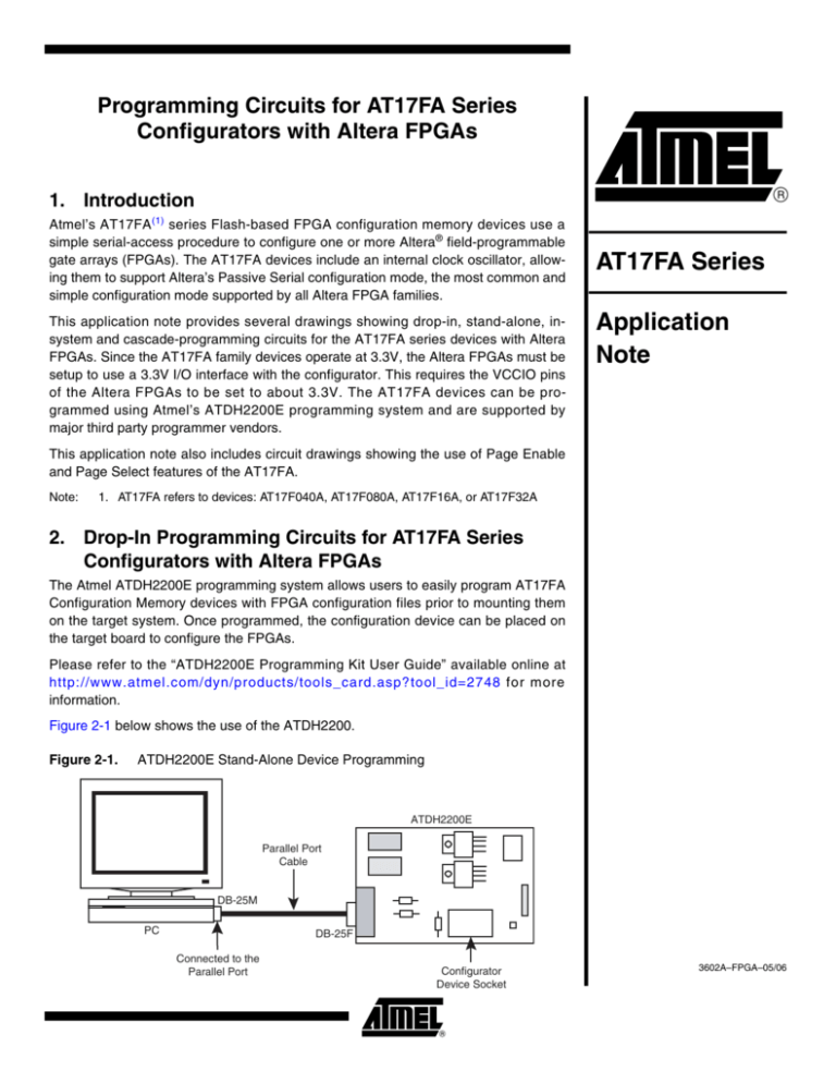
The Atmel ATDH2200E programming system allows users to easily program AT17FA
Configuration Memory devices with FPGA configuration files prior to mounting them
on the target system. Once programmed, the configuration device can be placed on
the target board to configure the FPGAs.
Please refer to the “ATDH2200E Programming Kit User Guide” available online at
http://www.atmel.com/dyn/products/tools_card.asp?tool_id=2748 for more
information.
Figure 2-1 below shows the use of the ATDH2200.
Figure 2-1.
ATDH2200E Stand-Alone Device Programming
ATDH2200E
Parallel Port
Cable
DB-25M
PC
DB-25F
Connected to the
Parallel Port
Configurator
Device Socket
3602A–FPGA–05/06
In addition to the ATDH2200E programming system, many third-party programmers support the
AT17FA Flash memory devices. A list of third-party programmer vendors supporting Atmel products can be found at: http://www.atmel.com/products/Config/thirdparty.asp. Please contact the
programmer vendors for support availability.
Figure 2-2 below shows all the required connections between the AT17FA configurator and an
Altera FPGA device when in-system programming is not required. This circuit requires that the
AT17FA device be programmed either by the ATDH2000E programming system or a third-party
programmer prior to mounting or using with target FPGA.
Figure 2-2.
Drop-In circuit showing an AT17FA Series Device with an Altera FPGA
CycloneTM I, II
Stratix® I, II
Stratix GX
FPGA
VCC(5)
VCC(5)
(4)
VCC(5)
VCC(5)
(4)
AT17FA
Configurator
(4)
nCONFIG
(2)
MSEL(3)
Pins
DATA0
DATA
DCLK
DCLK
nCS
CONF_DONE
SER_EN
PAGE_EN
PAGESEL[1:0]
RESET/OE
nSTATUS
nCE
nCASC/A2
READY(1)
(6)
GND
Notes:
1. Use of the READY pin is optional.
2. 0.1 µF capacitor is optional. If READY is not connected, an RC filter is recommended for input
to nCONFIG to delay configuration until VCC is stable. nCONFIG can instead be connected to
an active-low system reset signal.
3. MSEL pins should set the FPGA in the Passive Serial (PS) mode. For more detailed information, refer to the appropriate FPGA datasheet.
4. 10K Ohm
5. VCC = 3.3V
6. 100 pF capacitor
2
AT17FA Series Application Note
3602A–FPGA–05/06
AT17FA Series Application Note
3. In-System Programming Setup for AT17FA Series Configurators with Altera
FPGAs
To perform In-System Programming (ISP), the ATDH2225 programming dongle is required in
order to provide communication between the PC and the configurator targeted for programming.
See Figure 3-1.
Figure 3-1.
ATDH2225 In-System Programming Setup
AT17FA Series
Device
10-pin
Ribbon
Cable
Target System
FPGA
ATDH2225
PC
10
Connected to
Parallel Port
Programming
Dongle
In-System
Programming
Connector
10-pin Header
3
3602A–FPGA–05/06
4. In-System Programming Circuits for AT17FA Series Configurators with Altera
FPGAs
Figure 4-1 below shows all the required connections between the AT17FA Configurator, ISP circuits, and a single Altera FPGA device.
Figure 4-1.
In-System Programming Circuit of AT17FA Series Devices with an Altera FPGA
VCC(5)
10-pin
VCC(5) VCC(5)
Header
(4)
Cyclone I, II
Stratix I, II
Stratix GX
FPGA
VCC(5)
(4)
1
3
5
7
9
VCC(5) VCC(5)
(4)
(4)
(4)
AT17FA
Configurator
nCONFIG
(2)
2
4
6
8
10
DATA0
MSEL(6)
Pins
SER_EN
DATA
DCLK
DCLK
nCS
CONF_DONE
PAGE_EN
PAGESEL[1:0]
nCASC/A2(3)
RESET/OE
nSTATUS
nCE
READY(1)
(7)
Notes:
1. Use of the READY pin is optional.
2. 0.1 µF capacitor. If READY is used, the 0.1 µF capacitor is not needed. If READY is not connected, an RC filter is recommended for input to nCONFIG to delay configuration until VCC is
stable. nCONFIG can instead be connected to an active-low system reset signal.
3. The A2 bit-level setting in the Configurator Programming System (CPS) software should match
the A2 pin setting in the hardware. By default, it must be set to high for ISP access to Series
Device 1 and set to low for Series Device 2.
4. 10K Ohm
5. VCC = 3.3V
6. MSEL pins should set the FPGA in the Passive Serial (PS) mode. For more detailed information, refer to the appropriate FPGA datasheet.
7. 100 pF capacitor
4
AT17FA Series Application Note
3602A–FPGA–05/06
AT17FA Series Application Note
Figure 4-2.
In-System-Programming of a Single AT17FA Series Device with Cascaded Altera
FPGAs
VCC(5)
10-pin
VCC(5) VCC(5)
Header
(4)
Cyclone I, II
Stratix I, II
Stratix GX
FPGA
VCC(5)
(4)
1
3
5
7
9
VCC(5) VCC(5)
(4)
(4)
(4)
AT17FA
Series Device 1
nCONFIG
(2)
2
4
6
8
10
DATA0
MSEL(6)
Pins
SER_EN
DATA
DCLK
DCLK
nCS
CONF_DONE
PAGE_EN
PAGESEL[1:0]
nCASC/A2(3)
RESET/OE
nSTATUS
nCE
READY(1)
(7)
AT17FA
Series Device 2
SER_EN
DATA
DCLK
nCS
PAGE_EN
PAGESEL[1:0]
nCASC/A2(3)
RESET/OE
Notes:
READY(1)
1. Use of the READY pin is optional.
2. 0.1 µF capacitor. If READY is used, the 0.1 µF capacitor is not needed. If READY is not connected, an RC filter is recommended for input to nCONFIG to delay configuration until VCC is
stable. nCONFIG can instead be connected to an active-low system reset signal.
3. The A2 bit-level setting in the Configurator Programming System (CPS) software should match
the A2 pin setting in the hardware. By default, it must be set to high for ISP access to Series
Device 1 and set to low for Series Device 2.
4. 10K Ohm
5. VCC = 3.3V
6. MSEL pins should set the FPGA in the Passive Serial (PS) mode. For more detailed information, refer to the appropriate FPGA datasheet.
7. 100 pF capacitor
5
3602A–FPGA–05/06
5. Cascaded Programming Circuits using AT17FA Series Configurators with
Altera FPGAs
AT17FA devices provide a feature that allows a large FPGA configuration file that will not fit into
one configurator device to be stored and downloaded from two AT17FA devices in serial cascade fashion.
When performing in-system programming with cascaded configurators, special attention must
be given to the CEO/A2 I/O pins of the two configurator devices. While in configurator programming mode, (SEREN = 0), the CEO/A2 pins act as address line input A2. Consequently, in order
for the ISP software to individually communicate with each device, each device must have a different address setting. In Figure 5-1, Device 1 uses its internal pull-up resister to provide the
logic “1” setting to its A2 pin, while the A2 pin of Device 2 is connected to ground for logic “0”.
Hence, each configurator responds only to ISP software messages bearing its unique address.
Figure 5-1.
In-System Programming of cascaded AT17FA Series Devices with Single Altera
FPGA
VCC(5)
10-pin
VCC(5) VCC(5)
Header
(4)
Cyclone I, II
Stratix I, II
Stratix GX
FPGA
VCC(5)
VCC(5) VCC(5)
(4)
Device 1
(4)
1
3
5
7
9
AT17FA
Configurator
DATA0
MSEL(6)
Pins
SER_EN
DATA
DCLK
DCLK
nCS
CONF_DONE
nCEO
(4)
(4)
nCONFIG
(2)
2
4
6
8
10
PAGE_EN
PAGESEL[1:0]
nCASC/A2(3)
RESET/OE
nSTATUS
nCE
READY(1)
(7)
GND
Device 2
nCONFIG
nCE
NC
6
DATA0
DCLK
MSEL(6) CONF_DONE
Pins
nSTATUS
nCEO
AT17FA Series Application Note
3602A–FPGA–05/06
AT17FA Series Application Note
Notes:
1. Use of the READY pin is optional.
2. 0.1 µF capacitor. If READY is used, the 0.1 µF capacitor is not needed. If READY is not connected, an RC filter is recommended for input to nCONFIG to delay configuration until VCC is
stable. nCONFIG can instead be connected to an active-low system reset signal.
3. The A2 bit-level setting in the Configurator Programming System (CPS) software should match
the A2 pin setting in the hardware. By default, it must be set to high for ISP access to Series
Device 1 and set to low for Series Device 2.
4. 10K Ohm
5. VCC = 3.3V
6. MSEL pins should set the FPGA in the Passive Serial (PS) mode. For more detailed information, refer to the appropriate FPGA datasheet.
7. 100 pF capacitor
Figure 5-2.
In-System Programming of cascaded AT17FA Series Devices with Cascaded
Altera FPGAs
VCC(5)
10-pin
VCC(5) VCC(5)
Header
(4)
Cyclone I, II
Stratix I, II
Stratix GX
FPGA
VCC(5)
Device 1
(4)
1
3
5
7
9
VCC(5) VCC(5)
(4)
AT17FA
Series Device 1
DATA0
MSEL(6)
Pins
DCLK
DCLK
nCS
PAGE_EN
PAGESEL[1:0]
nCASC/A2(3)
RESET/OE
nSTATUS
nCE
SER_EN
DATA
CONF_DONE
nCEO
(4)
(4)
nCONFIG
(2)
2
4
6
8
10
(7)
GND
AT17FA
Series Device 2
Device 2
nCE
NC
SER_EN
DATA
nCONFIG
DATA0
DCLK
MSEL(6) CONF_DONE
Pins
nSTATUS
nCEO
DCLK
nCS
PAGE_EN
PAGESEL[1:0]
nCASC/A2(3)
RESET/OE
READY(1)
7
3602A–FPGA–05/06
Notes:
1. Use of the READY pin is optional.
2. 0.1 µF capacitor. If READY is used, the 0.1 µF capacitor is not needed. If READY is not connected, an RC filter is recommended for input to nCONFIG to delay configuration until VCC is
stable. nCONFIG can instead be connected to an active-low system reset signal.
3. The A2 bit-level setting in the Configurator Programming System (CPS) software should match
the A2 pin setting in the hardware. By default, it must be set to high for ISP access to Series
Device 1 and set to low for Series Device 2.
4. 1K Ohm
5. VCC = 3.3V
6. MSEL pins should set the FPGA in the Passive Serial (PS) mode. For more detailed information, refer to the appropriate FPGA datasheet.
7. 100 pF capacitor
6. Using the Multiple Configuration Page Capabilities of AT17FA Configurators
AT17FA configurators provide a memory page feature that allows users to store four configuration files at four different page locations and instantly configure their FPGA device with the
functionality given by each bitstream.
As an example of its usefulness, designs requiring a 1M-bit configuration device may benefit
from using the AT17F040A since up to four different configurations can be stored and accessed
as needed. This will simplify field upgrades and parts inventory by reducing the need for four
1M-bit devices holding 4 different design implementations, to just one 4M-bit device with four different configurations.
When the PAGE_EN(1) input of the AT17FA device is set to logic “1”, the storage space of the
AT17FA device is split into four equal size partitions. Upon initiating a FPGA configuration
sequence, the configuration bitstream residing at the page given by the Pagesel [1:0] bits, will be
downloaded into the FPGA.
CPS software version 8.05 or later can be used to select and program the individual bitstreams
at the page locations the user desires. Alternatively, designers who choose to write there own
ISP code should note the address page boundaries as shown in Table 6-1.
Additional details on the use of the memory page feature and exact address boundary locations(2) can be found in the corresponding AT17FA device datasheet.
Table 6-1.
AT17FA Address Boundaries
PAGE_EN
PAGESEL
[1:0]
PAGE
AT17F040A
ADDR RANGE
AT17F080A
ADDR RANGE
AT17F16A
ADDR RANGE
AT17F32A
ADDR RANGE
0
XX
1-4
00000-3FFFF
00000-7FFFF
00000-FFFFF
000000-1FFFFF
1
00
1
00000-0FFFF
00000-1FFFF
00000-3FFFF
000000-07FFFF
1
01
2
10000-1FFFF
20000-3FFFF
40000-7FFFF
080000-0FFFFF
1
10
3
20000-2FFFF
40000-5FFFF
80000-BFFFF
100000-17FFFF
1
11
4
30000-3FFFF
60000-7FFFF
C0000-FFFFF
180000-1FFFFF
Figures 6-1 and 7-1 show circuit drawings, implementing the page enable and page select features of AT17FA devices. Use of the page feature is aided by control logic such as a microcontroller, PLD or DIP switch for the purpose of controlling the page selection pins.
Notes:
1. The page enable feature is not available on the low 8-lead LAP package
2. The address ranges reflect that data is stored 16-bits per address.
8
AT17FA Series Application Note
3602A–FPGA–05/06
AT17FA Series Application Note
Figure 6-1.
PLD/Microcontroller Logic Controlled Page Selection
VCC(5)
10-pin
VCC(5) VCC(5)
Header
(4)
Cyclone I, II
Stratix I, II
Stratix GX
FPGA
VCC(5)
(4)
1
3
5
7
9
VCC(5) VCC(5)
(4)
(4)
(4)
AT17FA
Configurator
nCONFIG
(2)
2
4
6
8
10
DATA0
MSEL(6)
Pins
DCLK
DCLK
nCS
CONF_DONE
PAGE_EN
PAGESEL[1:0]
nCASC/A2(3)
RESET/OE
nSTATUS
nCE
SER_EN
DATA
READY(1)
(7)
External Controller
(Microcontroller/PLD)
Notes:
1. Use of the READY pin is optional.
2. 0.1 µF capacitor. If READY is used, the 0.1 µF capacitor is not needed. If READY is not connected, an RC filter is recommended for input to nCONFIG to delay configuration until VCC is
stable. nCONFIG can instead be connected to an active-low system reset signal.
3. The A2 bit-level setting in the Configurator Programming System (CPS) software should match
the A2 pin setting in the hardware. By default, it must be set to high for ISP access to Series
Device 1 and set to low for Series Device 2.
4. 1K Ohm
5. VCC = 3.3V
6. MSEL pins should set the FPGA in the Passive Serial (PS) mode. For more detailed information, refer to the appropriate FPGA datasheet.
7. 100 pF capacitor
9
3602A–FPGA–05/06
7. How to Generate a Programming File for AT17FA Series Devices to be Used in
Altera FPGA Applications
To program Atmel AT17FA series devices for configuring Altera FPGAs in Passive Serial (PS)
mode, the user can export a compressed or decompressed raw binary file (.rbf) programming
file from Altera’s Quartus® II software.
In Quartus, the user can go to the “Assignments” manual > “Device” > “Device & Pin Options” >
“programming files” > Raw binary file (*.rbf) to generate the RBF for targeting an EPC series
device.
The following describes the steps to setup the compression option in Quartus II for generating
the programming file:
1. Go to “Assignments” > “Device” from the main menu of Quartus II.
2. In the main “Settings” window, click on the “Device & Pin Options” button.
3. In the “Device & Pin Options” window, select the “Configuration” tab.
4. For the “Configuration Scheme” field, select “Passive Serial (can use Configuration
Device)”.
5. In the “Configuration Device” section, select “EPC2”, “EPC4”, “EPC8”, or “EPC16”.
Notes:
1. The programming file for targeting EPC16 with compression can be used for AT17F32A.
The programming file for targeting EPC8 with compression can be used for AT17F16A.
The programming file for targeting EPC4 with compression can be used for AT17F080A.
The programming file for targeting EPC2 with compression can be used for AT17F040A.
2. The configuration bit of an Altera FPGA can be used to determine the density of the Atmel
AT17FA series configuration memory that can be used.
6. Check the “Generate compressed bitstreams” option.
7. Click on the “Configuration Device Options” button.
8. In the “Configuration Device Options” window, check the “Compression mode” option.
9. Clock “OK” three times to close all windows and return to the Quartus main menu.
Note:
Atmel AT17FA configurators do not have a decompression feature. However, there are two types
of decompression used for Altera FPGA configuration. One decompression type is done by Altera
enhanced configuration memory and the other type is done by an Altera FPGA during configuration which is used in the above mentioned case.
To disable compression for generating the normal programming file, both the “Generate compressed bitstreams” and “Compression mode” options should be unchecked in Quartus.
1. Go to “Assignments” > “Device” from the Quartus main menu.
2. In the main “Settings” window, click on the “Device & Pin Options” button.
3. In the “Device & Pin Options” window, select the “Configuration” tab.
4. For the “Configuration scheme” field, select “Active Serial (can use Configuration
Device)”.
5. In the “Configuration device” section, select “EPC4”, “EPC8” or “EPC16”.
6. Check the “Generate compressed bitstreams” options.
Notes:
1. The programming file for targeting EPC16 without compression can be used for AT17F16A.
The programming file for targeting EPC8 without compression can be used for AT17F080A.
The programming file for targeting EPC4 without compression can be used for AT17F040A.
2. The configuration bit of an Altera FPGA can be used to determine the density of the Atmel
AT17FA series configuration memory that can be used.
3. The programming file cannot be generated by selecting the EPCS family of the configuration
memories (EPCS1, EPCS4, EPCS16) for targeting the AT17FA series devices since SPI Flash
instructions are not supported by AT17FA series devices.
10
AT17FA Series Application Note
3602A–FPGA–05/06
AT17FA Series Application Note
If the Atmel ATDH2200E or ATDH2225 programming hardware is used, the RBF file can be
directly programmed to the device with the “/A” procedure in the Atmel CPS software. However,
if a third-party programmer is used, the user must use the .rbf file with the “/B” procedure in the
Atmel CPS software to convert it to a .hex file first (if two hex files are generated, only the first
hex file is used). For file conversion, the input file is .rbf and the output file is .bst. The .hex file
(Intel® MCS®-86 hex object file) will be generated at the same time.
The converted hex file can program as an Intel MCS86 hex object file to an Atmel AT17FA
device using any third-party programmer that supports AT17FA devices.
Atmel
CPS
software
can
be
downloaded
from
http://www.atmel.com/dyn/products/tools_card.asp?tool_id=3191.
Figure 7-1.
the
Atmel
at
Manually-Controlled Paging Selection
VCC(5)
10-pin
VCC(5) VCC(5)
Header
(4)
Cyclone I, II
Stratix I, II
Stratix GX
FPGA
VCC(5)
(4)
1
3
5
7
9
VCC(5) VCC(5)
(4)
(4)
(4)
AT17FA
Configurator
nCONFIG
(2)
2
4
6
8
10
DATA0
DATA
DCLK
DCLK
MSEL(6)
Pins
nCS
CONF_DONE
PAGE_EN
PAGESEL[1:0]
nCASC/A2(3)
RESET/OE
nSTATUS
nCE
SER_EN
READY(1)
(7)
2
VCC(5) VCC(5) VCC(5)
(4)
Notes:
(4)
(4)
DIP
Switches
1. Use of the READY pin is optional.
2. 0.1 µF capacitor. If READY is used, the 0.1 µF capacitor is not needed. If READY is not connected, an RC filter is recommended for input to nCONFIG to delay configuration until VCC is
stable. nCONFIG can instead be connected to an active-low system reset signal.
3. The A2 bit-level setting in the Configurator Programming System (CPS) software should match
the A2 pin setting in the hardware. By default, it must be set to high for ISP access to Series
Device 1 and set to low for Series Device 2.
4. 1K Ohm
5. VCC = 3.3V
6. MSEL pins should set the FPGA in the Passive Serial (PS) mode. For more detailed information, refer to the appropriate FPGA datasheet.
7. 100 pF capacitor
11
3602A–FPGA–05/06
Atmel Corporation
2325 Orchard Parkway
San Jose, CA 95131, USA
Tel: 1(408) 441-0311
Fax: 1(408) 487-2600
Regional Headquarters
Europe
Atmel Sarl
Route des Arsenaux 41
Case Postale 80
CH-1705 Fribourg
Switzerland
Tel: (41) 26-426-5555
Fax: (41) 26-426-5500
Asia
Room 1219
Chinachem Golden Plaza
77 Mody Road Tsimshatsui
East Kowloon
Hong Kong
Tel: (852) 2721-9778
Fax: (852) 2722-1369
Japan
9F, Tonetsu Shinkawa Bldg.
1-24-8 Shinkawa
Chuo-ku, Tokyo 104-0033
Japan
Tel: (81) 3-3523-3551
Fax: (81) 3-3523-7581
Atmel Operations
Memory
2325 Orchard Parkway
San Jose, CA 95131, USA
Tel: 1(408) 441-0311
Fax: 1(408) 436-4314
RF/Automotive
Theresienstrasse 2
Postfach 3535
74025 Heilbronn, Germany
Tel: (49) 71-31-67-0
Fax: (49) 71-31-67-2340
Microcontrollers
2325 Orchard Parkway
San Jose, CA 95131, USA
Tel: 1(408) 441-0311
Fax: 1(408) 436-4314
La Chantrerie
BP 70602
44306 Nantes Cedex 3, France
Tel: (33) 2-40-18-18-18
Fax: (33) 2-40-18-19-60
ASIC/ASSP/Smart Cards
1150 East Cheyenne Mtn. Blvd.
Colorado Springs, CO 80906, USA
Tel: 1(719) 576-3300
Fax: 1(719) 540-1759
Biometrics/Imaging/Hi-Rel MPU/
High-Speed Converters/RF Datacom
Avenue de Rochepleine
BP 123
38521 Saint-Egreve Cedex, France
Tel: (33) 4-76-58-30-00
Fax: (33) 4-76-58-34-80
Zone Industrielle
13106 Rousset Cedex, France
Tel: (33) 4-42-53-60-00
Fax: (33) 4-42-53-60-01
1150 East Cheyenne Mtn. Blvd.
Colorado Springs, CO 80906, USA
Tel: 1(719) 576-3300
Fax: 1(719) 540-1759
Scottish Enterprise Technology Park
Maxwell Building
East Kilbride G75 0QR, Scotland
Tel: (44) 1355-803-000
Fax: (44) 1355-242-743
Literature Requests
www.atmel.com/literature
Disclaimer: The information in this document is provided in connection with Atmel products. No license, express or implied, by estoppel or otherwise, to any
intellectual property right is granted by this document or in connection with the sale of Atmel products. EXCEPT AS SET FORTH IN ATMEL’S TERMS AND CONDITIONS OF SALE LOCATED ON ATMEL’S WEB SITE, ATMEL ASSUMES NO LIABILITY WHATSOEVER AND DISCLAIMS ANY EXPRESS, IMPLIED OR STATUTORY
WARRANTY RELATING TO ITS PRODUCTS INCLUDING, BUT NOT LIMITED TO, THE IMPLIED WARRANTY OF MERCHANTABILITY, FITNESS FOR A PARTICULAR
PURPOSE, OR NON-INFRINGEMENT. IN NO EVENT SHALL ATMEL BE LIABLE FOR ANY DIRECT, INDIRECT, CONSEQUENTIAL, PUNITIVE, SPECIAL OR INCIDENTAL DAMAGES (INCLUDING, WITHOUT LIMITATION, DAMAGES FOR LOSS OF PROFITS, BUSINESS INTERRUPTION, OR LOSS OF INFORMATION) ARISING OUT
OF THE USE OR INABILITY TO USE THIS DOCUMENT, EVEN IF ATMEL HAS BEEN ADVISED OF THE POSSIBILITY OF SUCH DAMAGES. Atmel makes no
representations or warranties with respect to the accuracy or completeness of the contents of this document and reserves the right to make changes to specifications
and product descriptions at any time without notice. Atmel does not make any commitment to update the information contained herein. Unless specifically provided
otherwise, Atmel products are not suitable for, and shall not be used in, automotive applications. Atmel’s products are not intended, authorized, or warranted for use
as components in applications intended to support or sustain life.
© 2006, Atmel Corporation. All rights reserved. Atmel ®, logo and combinations thereof, Everywhere You Are ® and others are registered
trademarks or trademarks of Atmel Corporation or its subsidiaries. Other terms and product names may be trademarks of others.
3602A–FPGA–05/06


