FPGA implementation of Decimal Adder and Multipliers in Binary
advertisement
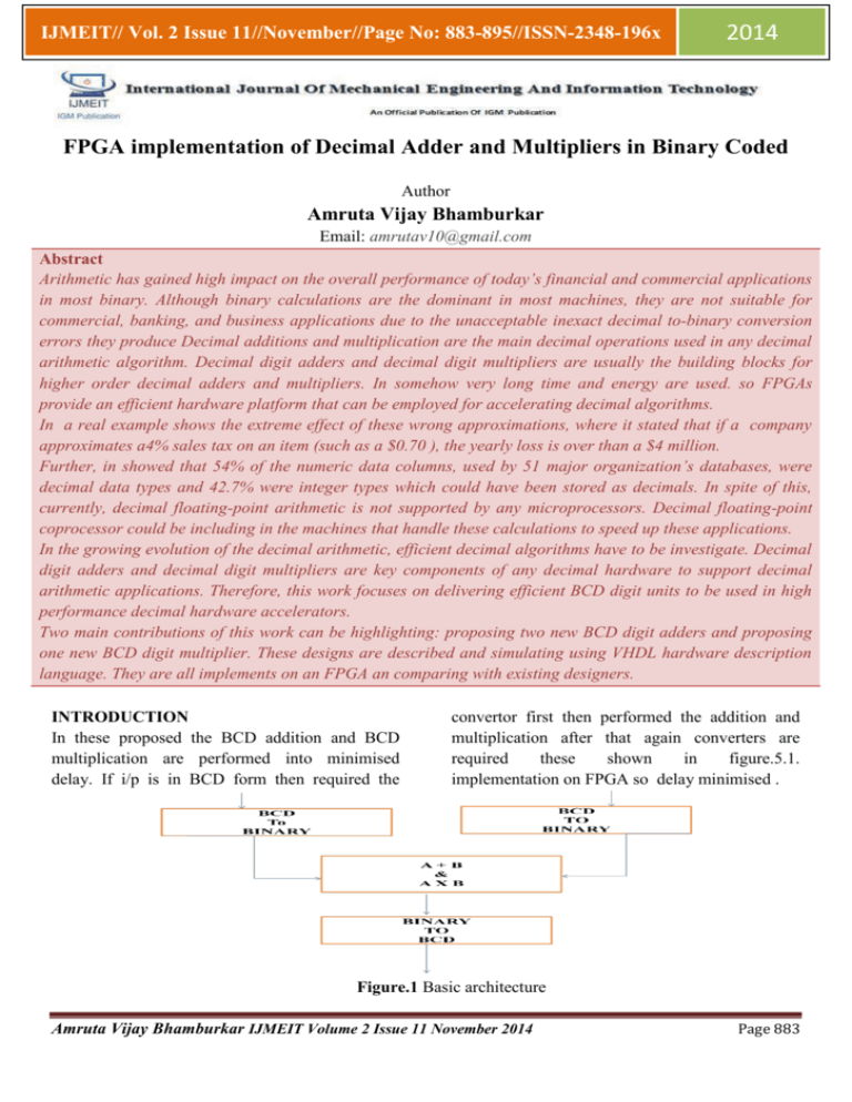
IJMEIT// Vol. 2 Issue 11//November//Page No: 883-895//ISSN-2348-196x 2014 FPGA implementation of Decimal Adder and Multipliers in Binary Coded Author Amruta Vijay Bhamburkar Email: amrutav10@gmail.com Abstract Arithmetic has gained high impact on the overall performance of today’s financial and commercial applications in most binary. Although binary calculations are the dominant in most machines, they are not suitable for commercial, banking, and business applications due to the unacceptable inexact decimal to-binary conversion errors they produce Decimal additions and multiplication are the main decimal operations used in any decimal arithmetic algorithm. Decimal digit adders and decimal digit multipliers are usually the building blocks for higher order decimal adders and multipliers. In somehow very long time and energy are used. so FPGAs provide an efficient hardware platform that can be employed for accelerating decimal algorithms. In a real example shows the extreme effect of these wrong approximations, where it stated that if a company approximates a4% sales tax on an item (such as a $0.70 ), the yearly loss is over than a $4 million. Further, in showed that 54% of the numeric data columns, used by 51 major organization’s databases, were decimal data types and 42.7% were integer types which could have been stored as decimals. In spite of this, currently, decimal floating-point arithmetic is not supported by any microprocessors. Decimal floating-point coprocessor could be including in the machines that handle these calculations to speed up these applications. In the growing evolution of the decimal arithmetic, efficient decimal algorithms have to be investigate. Decimal digit adders and decimal digit multipliers are key components of any decimal hardware to support decimal arithmetic applications. Therefore, this work focuses on delivering efficient BCD digit units to be used in high performance decimal hardware accelerators. Two main contributions of this work can be highlighting: proposing two new BCD digit adders and proposing one new BCD digit multiplier. These designs are described and simulating using VHDL hardware description language. They are all implements on an FPGA an comparing with existing designers. INTRODUCTION In these proposed the BCD addition and BCD multiplication are performed into minimised delay. If i/p is in BCD form then required the convertor first then performed the addition and multiplication after that again converters are required these shown in figure.5.1. implementation on FPGA so delay minimised . Figure.1 Basic architecture Amruta Vijay Bhamburkar IJMEIT Volume 2 Issue 11 November 2014 Page 883 IJMEIT// Vol. 2 Issue 11//November//Page No: 883-895//ISSN-2348-196x 1 ADDER The main problem in decimal addition, that increases the delay, is the need for correction if the result exceeds the permitted BCD range (decimal number 9). This correction actually adds the binary number (0110)2 to the result. In this project proposed design new high-speed areaoptimized correction-free BCD digit adders that can be employed in different decimal applications. Throughout this chapter, two new different design configurations for BCD digit adders are discussed. 1.1 DIFFERENT ARCHITECTURES The basic Adder Architectures are studied to design BCD Adder Configuration. In electronics, an adder or summer is a digital circuit that performs addition of numbers. In many computers and other kinds of processors, adders are used not only in the arithmetic logic unit(s), but also in other parts of the processor, where they are used to calculate addresses, table indices, and similar operations. Although adders can be constructed for many numerical representations, such as binary-coded decimal or excess-3, the most common adders operate on binary numbers. In cases where two's complement or ones' complement is being used to represent negative numbers, it is trivial to modify an adder into an adder–sub tractor. Other signed number representations require a more complex adder. a) HALF ADDER Figure.2 half adder The half adder adds two single binary digits A and B. It has two outputs, sum (S) and carry (C). The carry signal represents an overflow into the next digit of a multi-digit addition. The value of the sum is 2C + S. The simplest half-adder design, 2014 pictured on the right, incorporates an XOR gate for S and an AND gate for C. With the addition of an OR gate to combine their carry outputs, two half adders can be combined to make a full adder. The half-adder adds two input bits and generates a carry and sum, which are the two outputs of halfadder. The input variables of a half adder are called the augend and addend bits. The output variables are the sum and carry. b) FULL ADDER Figure 3 full adder A full adder can be implemented in many different ways such as with a custom transistorlevel circuit or composed of other gates. One example implementation is with and . In this implementation, the final OR gate before the carry-out output may be replaced by an XOR gate without altering the resulting logic. Using only two types of gates is convenient if the circuit is being implemented using simple IC chips which contain only one gate type per chip. The carryblock subcomponent consists of 2 gates and therefore has a delay of In the variety adder are used. Each type of adder are selected on the where are used basic adder A combinational circuit that adds two bits is called a half adder A full adder is one that adds three bits, the third produced from a previous addition operation basically the following adder are used in VLSI we consider, Amruta Vijay Bhamburkar IJMEIT Volume 2 Issue 11 November 2014 Page 884 IJMEIT// Vol. 2 Issue 11//November//Page No: 883-895//ISSN-2348-196x 1. Ripple carry adder 2. Carry look head adder 1. Ripple Carry Adder: The ripple carry adder is constructed by cascading full adder blocks in series. The carryout of one stage is fed directly to the carry-in of the next 2014 stage For an n-bit parallel adder, it requires n full adders .is shown in the figure.4. In these calculated the carry by one by one then total time have to be consider. When n bit consider then carry calculation are complex. Figure 4: Ripple carry adder Drawback: 1. not very efficient in large bit number are used. 2 .delay increase linearly with bit rate 2. Carry look head adder: Ripple carry adder drawback overcome by carry look head adder. Carry Look Ahead Adder (CLA) has a proper balance between both the Area occupied and Time required. Hence among the three, Carry Look Ahead Adder has the least AREA DELAY PRODUCT. Hence we should use Carry Look ahead Adders when it comes to optimization with both Area and Time. For an instance, the last stage of the Wallace tree Adder in Booth multiplier is a Carry look Ahead Adder. In these Calculates the carry signals in advance, based on the input signals generator carry look ahead adder is shown in figure 5. Boolean Equations Pi = Ai +Bi Carry propagate Gi = Ai Bi Carry generate Si = Pi Ci Sum Ci+1= Gi + PiC Carry out Signals P and G only depend on the input bits, Applying these equations for a 4-bit adder: C1 = G0 + P0C0 C2 = G1 + P1C1 = G1 + P1(G0 + P0C0) = G1 + P1G0 + P1P0C0 C3 = G2 + P2C2 = G2 + P2G1 + P2P1G0 + P2P1P0C0 C4 = G3 + P3C3 = G3 + P3G2 + P3P2G1 + P3P2P1G0 + P3P2P1P0C0 Figure .5 :Look ahead carry generator Amruta Vijay Bhamburkar IJMEIT Volume 2 Issue 11 November 2014 Page 885 IJMEIT// Vol. 2 Issue 11//November//Page No: 883-895//ISSN-2348-196x 2014 Advantage of carry look ahead adder that they have consider direct carry. they give the minimum delay, Because of that it very efficient in the large bit number. 3. BCD Adder Design a direct BCD digit adder using a four bit input, five bit output combinational logic. The four bit inputs are the two BCD input digits A and B plus the decimal carry input Cin and the five bit outputs are the BCD digit of the decimal sum S plus the decimal carry out Cout. For example, to add (6 + 7 = 13), this operation is translated to (0110 + 0111 = 10011) BCD. The output result (10011) BCD is the BCD representation of the decimal number 13. The most significant bit is the decimal carry output generated from the addition operation, while the other bits are the BCD summation digit. The truth table for all output logic functions is constructed for all possible combinations of the inputs. Since the inputs are nine bits, the number of possible combinations is 24 = 16. Many of these combinations are valid since 4-bit number can take any value from 0 to (15)10. In the case when the input is not valid, the output is set to don’t care. The two input BCD digits are assumed to be A = a3a2a1a0 and B = b3b2b1b0. The output consists of the BCD digit sum S = s3s2s1s0 and the decimal carry output. This adder is designed to support both binary and decimal additions. A binary carry look-ahead adder (CLA) is used to add two input operands, which are either binary or decimal numbers. The result of the binary CLA is the correct result for binary inputs, but it needs to be corrected for decimal inputs. This proposed architecture requires less area compared to other configurations. Figure .6 BCD adder architecture The first adder configuration is the conventional decimal adder. For each decimal digit, it has two 4-bit binary adders and correction circuit between the adders. The first level adders produce the binary addition results. If the result is greater than 9, a carry output is produced and the result of first level 4-bit adder is corrected by adding 6. Furthermore, the carry output is used as a carry input for the next digit. The main advantage of the direct Boolean expression BCD adder is its area reduction. 1.2 Multipliers Multiplication is one of the basic arithmetic operations and it requires substantially more hardware resources and processing time. In the decimal system, digit-by-digit lookup table multipliers are inefficient from both area and speed sides. There are number of techniques that can be used to perform multiplication. In general, the choice is based upon factors such as latency, throughput, area, and design complexity. More efficient approach uses some sort of array or tree of full adders to sum partial products. Array multiplier, Wallace Tree multipliers are suitable for VLSI implementation. Multipliers are key components of many high performance systems such as FIR filters, Amruta Vijay Bhamburkar IJMEIT Volume 2 Issue 11 November 2014 Page 886 IJMEIT// Vol. 2 Issue 11//November//Page No: 883-895//ISSN-2348-196x microprocessors, digital signal processors, etc. A system’s performance is generally determined by the performance of the multiplier because the multiplier is generally the lowest element in the system. Furthermore, it is generally the most area consuming. Hence, optimizing the speed and area of the multiplier is a major design issue. However, area and speed are usually conflicting constraints so that improving speed results mostly in larger areas. 1.2.1 ARRAY MULTIPLIER Array multiplier is an efficient layout of a combinational multiplier. Multiplication of two binary number can be obtained with one microoperation by using a combinational circuit that forms the product bit all at once thus making it a fast way of multiplying two numbers since only delay is the time for the signals to propagate through the gates that forms the multiplication array. A basic Array multiplier consists of three parts (i) partial product generation (ii) partial product addition and (iii) final addition. In Array multiplier, word “direct” means no need for neither “first finding the binary multiplication result and then converting the product to a BCD form” nor “any recoding process” .Instead, we 2014 have used a simplified Boolean expressions to perform the “direct” functionality. In this case, the two operands are two decimal digits A = a3a2a1a0 and B = b3b2b1b0 and the output P = A × B is 8 bit P7P6P5P4P3P2P1P0 (two BCD digits). Since the input is 8 bits wide, the number of combinations in the truth table is 28 = 256. Among all these combinations only 100 combinations are valid and the rest are invalid. All outputs for the invalid combinations in the truth table are set to don’t care. If the output functions depend on more than six variables from the input variable then it needs hierarchy of LUTs to be implemented. An example on this is P1 which depends on all the eight input variables. On the other hand, some functions depend only on two variables like P0 or four variables like P7. This means that these two outputs consumes a single 6-input LUT each. In array multiplier, consider two binary numbers A and B, of m and n bits. There are m n summands that are produced in parallel by a set of m n AND gates. n x n multiplier requires n (n-2) full adders, n half-adders and n2AND gates. Also, in array multiplier worst case delay would be (2n+1) td. multiplier worst case delay architecture of array multiplier shown in fig.7. . Figure.7 Archite acture of array multiplier Amruta Vijay Bhamburkar IJMEIT Volume 2 Issue 11 November 2014 Page 887 IJMEIT// Vol. 2 Issue 11//November//Page No: 883-895//ISSN-2348-196x Drawback of array multiplier 1. Array Multiplier gives more power consumption as well as optimum number of components required, but delay for this multiplier is larger. 2. It also requires larger number of gates because of which area is also increased; due to this array multiplier is less economical. Thus, it is a fast multiplier but hardware complexity is high. 1.2.2 WALLACE MULTIPLIER A fast process for multiplication of two numbers was developed by Wallace. Using this method, a three step process is used to multiply two numbers; the bit products are formed, the bit product matrix is reduced to a two row matrix where sum of the row equals the sum of bit products, and the two resulting rows are summed with a fast adder to produce a final product. In the Wallace tree method, three bit signals are passed to a one bit full adder (“3W”) which is called a three input Wallace tree circuit, and the output signal (sum signal) is supplied to the next stage full adder of the same bit, and the carry output signal is passed to the next stage full adder of the same no of bit, and the carry output signal is supplied to the next stage of the full adder located at a one bit higher position. Wallace tree is reducing the number of operands at earliest opportunity. 2014 A multiplier essentially consists of two operands, a multiplicand “A” and a multiplier “B” and produces a product “P”. In the first stage, the multiplicand and the multiplier are multiplied bit by bit to generate the partial product terms. The second stage is the most important, as it is the most complicated and determines the overall speed of the multiplier. This stage includes addition of these partial product terms to generate the product “P”. This paper will be more focused on the optimization of this stage, which consists of the addition of all the partial products. If speed is not an issue, the partial products can be added serially, reducing the design complexity. However, in high-speed design, the Wallace tree construction method is usually used to add the partial products in a tree-like fashion in order to produce two rows of partial products that can be added in the last stage. Fig.8.shows the structural representation of 4x4 multiplier using half adders and full adders for the addition of intermediate terms formed after the multiplication of two numbers. Finally, the product output is shown, showing each bit of the product obtained. R0 to R15 denotes the various product terms obtained at the first stage of multiplication. Product term a0b0 is represented by R0. Similarly the other product terms are represented by different notations from R1 to R15. Figure.8 Architecture of WALLACE MULTIPLIER Amruta Vijay Bhamburkar IJMEIT Volume 2 Issue 11 November 2014 Page 888 IJMEIT// Vol. 2 Issue 11//November//Page No: 883-895//ISSN-2348-196x The first bit p0 of the product P is obtained by the first product term a0b0 which is denoted by R0. R1 and R2 then become the inputs of the half adder to give two outputs, sum S1 and carry C1. Sum S1 is nothing but the next bit of the product P which is denoted by p1. R3, R4, and R5 become the input bits of the full adder to give outputs as sum S2 and carry C2. Previous carry C1 and sum S2 becomes the input bits of next half adder to produce two outputs sum S6 and carry C6. Sum S6 is the third bit of the product P which is named as p2. The remaining bits of the product P i.e. p3, p4, p5, p6, p7, p8 respectively are obtained in the same way as explained. 1.2.3 BCD MULTIPLIER `A Binary multiplier is an electronic hardware device used in digital electronics or a computer or other electronic device to perform rapid multiplication of two numbers in binary representation. Efficient BCD Multiplier is design by using the architecture of Wallace Tree. Wallace tree multiplier consists of three step process, in the first step, the bit product terms are formed after the multiplication of the bits of multiplicand and multiplier, in second step, the bit product matrix is reduced to lower number of rows using half and full adders, this process continues till the last addition remains, in the final step, final addition is done using adders to obtain the result. Figure. 9 multiplication of two numbers A and B 2014 Fig. 9 shows the multiplication of two numbers A and B and producing its result as P. explains the method of addition of different intermediate terms. The different intermediate terms formed after the multiplication of two 4-bit numbers. Two intermediate terms in one column are added using a half adder and more than two terms in one column are added using full adder as explained in fig.10. The sum obtained after each addition is denoted by where varies from 1 to 10. Similarly carries are denoted by where varies from 1 to 10 and denotes next carries, where varies from 0 to 3. Figure. 10 the method of addition of different intermediate terms Designing of BCD Digit Multiplier based on Wallace Tree Architecture uses a novel method, which has been proved to be more efficient i.e. shift and add-3 algorithm, to convert from binary to BCD. The effective combination of the new binary to BCD converter with the embedded binary multipliers in the FPGAs, has been shown to be competitive. The shift and add-3 algorithmic steps are as follows 1. Shift the binary number left one bit. 2. If 8 shifts have taken place, the BCD number is in the Hundreds, Tens and Units column. 3. If the binary value in any of the BCD columns is 5 or greater, add 3 to that value in that BCD column. 4. Go to 1. Amruta Vijay Bhamburkar IJMEIT Volume 2 Issue 11 November 2014 Page 889 IJMEIT// Vol. 2 Issue 11//November//Page No: 883-895//ISSN-2348-196x 2014 Finally BCD multiplier is designed to provide high performance & consumes less power. BCD digit multiplier gives the best speed performance. So, latency become smaller as speed and latency are inversely proportional to each other. SOFTWERS TOOL Model Sim SE 6.3f and simulation tool for VHDL, Verilog and mixed hardware descriptive languadesigns, used is ModelSim SE 6.3f software Xilinx ISE 13.1 Xilinx Integrated Software Environment (ISE) is a software tool developed by Xilinx corporation for the synthesis and analysis of Hardware Descriptive Language (HDL) designs. It enables the synthesis of designs, timing analysis, Register Transfer Level (RTL) diagram examinations and simulation as per different environments as well as the configuration of the target device with the help of the programmer DESIGN PROJECT FLOW CHART Figure. 11 design of project flow. From design specification, BCD adder and multiplier, design is coded using Very High Speed Integrated Circuit Hardware Descriptive Language. In a designed correction less BCD adder the logic of carry look ahead adder used, and BCD multiplier the Wallace multiplier logic are used. Simulation and verification is done on ModelSim SE 6.3f software. Results are then synthesized on Xilinx ISE 13.1. Finally, Figure.11 Design of Project Flow Observation 6.1 ADDER The main problem in decimal addition, that increases the delay, is the need for correction if the result exceeds the permitted BCD range (decimal number 9). This correction actually adds the binary number (0110)2 to the result. One contribution in this work is the design of new high-speed area-optimized correction-free BCD digit adders that can be employed in different decimal applications. 6.1.1 Ripple Carry Adder The ripple carry adder is constructed by cascading full adder blocks in series. The carryout of one stage is fed directly to the carry-in of the next stage For an n-bit parallel adder, it requires n full adders. simulation o/p are shown in figure.12 Amruta Vijay Bhamburkar IJMEIT Volume 2 Issue 11 November 2014 Page 890 IJMEIT// Vol. 2 Issue 11//November//Page No: 883-895//ISSN-2348-196x Simulation process : b =0001 the i/p are as, 2014 a=0010, Figure12 simulation for ripple carry adder b) Synthesis Process: In synthesis report ripple carry adder design is implemented separately on Xilinx XC3S500E Spartan-3E FPGA kit. we can calculated time that is the delay..and device summary are shown as follows Timing Summary: Maximum combinational path delay: 9.926ns * 4 = 39.704 ns Device utilization summary: Selected Device : 3s500efg320-4 a= 0011 b =0011 Number of Slices: 4 out of 4656 0% Number of 4 input LUTs: 8 out of 9312 0% Number of IOs: 14 Number of bonded IOBs: 14 out of 232 6% 6.1.2 Carry look head adder a) Simulation process : Ripple carry adder drawback over come by carry look head adder. In these Calculates the carry signals in advance, based on the input signals .the output are shown in fig 13 Figure 13 simulation process for carry look ahead adder b) Synthesise process: In synthesis design isimplemented separately on Xilinx XC3S500E Spartan-3E FPGA kit. calculated the delay, The maximum time required device summery are shown as Timing Summary: Maximum combinational path delay: 9.926ns Device utilization summary: Selected Device : 3s500efg320-4 Number of Slices: 4 out of 4656 0% Number of 4 input LUTs: 8 out of 9312 0% Number of IOs: 14 Number of bonded IOBs: 14 out of 232 6% 6.1.3 BCD Adder a) Simulation process : BCD addition by overall function done by procedure are done by step in these simulation. In Amruta Vijay Bhamburkar IJMEIT Volume 2 Issue 11 November 2014 Page 891 2014 IJMEIT// Vol. 2 Issue 11//November//Page No: 883-895//ISSN-2348-196x simulation ripple carry adder, carry look ahead adder, conversion programme are included . In these BCD adder when we have the BCD I/p then o/p is in also BCD so that binary to decimal are converted need in a ripple carry adder and carry look ahead adder are all these included and conversion programme. The i/p’s are 0111, 0110 as shown in figure14 1 Figure. 14 simulation process for bcd adder Number of Slices: 4 out of 4656 0% b) Synthesise process: In synthesis report number of logic utilised is Number of 4 input LUTs: 7 out of 9312 0% shown in fig bcd adder design is implemented Number of IOs: 40 separately on Xilinx XC3S500E Spartan-3E Number of bonded IOBs: 40 out of 232 17% FPGA kit. Timinge Summary: 6.1.4 Comparison: Maximum combinational path delay: 8.748ns Comparing the ripple carry adder , Carry look Device utilization summary: ahead adder, BCD adder in base of delay and area Selected Device : 3s500efg320-4 is shown in table no. 1 Different of adder Delay ( ns ) No. of LUT’s 9312 RCA 39.70 8 CLA 9.927 8 BCD 8.748 7 Table no. 1 show comparison of adder 6.2 MULTIPLIER Binary coded decimal digit multiplier is a fundamental cell in the BCD multiplication operation. It multiplies two BCD digits to produce a two BCD digits product output. In these proposed new BCD digit multiplier 6.2.1 Array multiplier a) Simulation process : Array multiplier is combination of half adder full adder and array programmed is included. In the i/p are a= 0011 b=0010 is shown in figure.15 Figure.15 imulation process of array multiplier Amruta Vijay Bhamburkar IJMEIT Volume 2 Issue 11 November 2014 Page 892 IJMEIT// Vol. 2 Issue 11//November//Page No: 883-895//ISSN-2348-196x b) Synthesise process: In synthesis report number of logic utilised is tabel no. 2. Arey multiplier 2014 design is implemented separately on Xilinx XC3S500E Spartan-3E FPGA kit. Table no 2 device utilization summary for Array Multiplier 6.2.2 WALLACE MULTIPLIER Wallace tree is reducing the number of operands at earliest opportunity. A) Simulation process : In i/p’s a = 0011, b = 0000 Figure. 16 Simulation process for WALLACE MULTIPLIER b) Synthesise process: In synthesis report number of logic utilised is shown in design is implemented separately on Xilinx XC3S500E Spartan-3E FPGA kit Table no3 device utilization summary for WALLACE MULTIPLIER latency become smaller as speed and latency are 6.2.3 BCD MULTIPLIER Efficient BCD Multiplier is design by using the inversely proportional to each other. architecture of Wallace Tree. Finally BCD a) Simulation process : In figure shows for i/p multiplier is designed to provide high mult.1= 0011 performance & consumes less power. BCD digit multiplier gives the best speed performance. So, Mult.2= 0011 Amruta Vijay Bhamburkar IJMEIT Volume 2 Issue 11 November 2014 Page 893 IJMEIT// Vol. 2 Issue 11//November//Page No: 883-895//ISSN-2348-196x 2014 Figure.17 Simulation process of BCD multiplier b) Synthesise process: In synthesis report number of logic utilised is shown in design is implemented separately on Xilinx XC3S500E Spartan-3E FPGA kit. Table no.4 device utilization summary for BCD multiplier 6.2.4 Comparisons: Comparison between Array multiplier ,Wallace multiplier and BCD of multiplier on the area and delay Different of Multiplier Delay (ns) Array mult. Wallace mult. BCD mult. No. Of LUT’s out of 9312 24.944 33 18.708 33 24.622 65 Table no.5 Comparison of different multiplier CHAPTER CONCLUSION 7.1 CONCLUSION All above proposed designs were described using VHDL hardware description language, and simulated to ensure correct functionality. They were synthesized with Xilinx ISE tool and then simulated in Modelsim Simulator SE . Synthesis results of our BCD digit adders & multipliers are shown in above. In this project, new BCD digit adders and one new BCD digit multipliers are designed to speed up decimal arithmetic applications over FPGA. The different designers have proposed several enhancements for high speed, area optimization. In proposed that implemented direct BCD Addition approach which provide correction-free addition techniques. In this project, the proposed Direct Boolean Expression BCD Digit Adder optimized the resource utilization factors. So, this configuration also defined as minimal area BCD Adder. Analysis & synthesis results show that our Amruta Vijay Bhamburkar IJMEIT Volume 2 Issue 11 November 2014 Page 894 IJMEIT// Vol. 2 Issue 11//November//Page No: 883-895//ISSN-2348-196x Correction free BCD digit adder is the fastest among other proposed adders and comparision of all are shown in table. The BCD Multiplier is implemented using Wallace Multipliers architecture which consumes less propagation time delay wrt the operations compared to other multipliers architecture. REFERENCES 1. REKHA K. JAMES and SHAHANA T. K, “Decimal Multiplication using compact BCD Multiplier ”, 2008 IEEE International Conference on Electronic Design. 2. Alvaro Vazquez, Elisardo Antelo, “Improved Design of High-Performance Parallel Decimal Multipliers ”,IEEE TRANSACTIONS ON COMPUTERS,MAY 2010 3. Álvaro Vázquez, “Multi-operand Decimal Adder Trees for FPGAs”, INRIA 14 Oct 201 4. L. Dadda ,“ A Parallel-Serial Decimal Multiplier Architecture” ,in 2012 IEEE 5. Osama D. Al-Khaleel, “FPGA implementation of Binary Coded Decimal Digit Adders and Multipliers”, IEEE (2012). 6. Kaivani, “Binary-coded decimal digit multipliers,” IET Computers and Digital 2014 Techniques, vol. 1, no. 4, pp. 377–381, 2007. 7. H. Wetter W. Bultmann, W. Haller and A. Worner, “Binary and decimal adder unit,” 2001. E. M. Schwarz, “Decimal multiplication with efficient partial product generation,” in Proceedings of the 17th IEEE Symposium on M. F. Cowlishaw, “Decimal floating-point: Algorism for computers,” in Proceedings of the 16th IEEE Symposium on Computer Arithmetic (ARITH-16’03), Washington, DC, USA, 2003, ARITH ’03, pp. 104– ,IEEE Computer Society. 8. Society. Arithmetic, Washington, DC, USA, 2005, ARITH ’05, pp. 21–28, IEEE Computer Society. 9. Vazquez, E. Antelo, and P. Montuschi, “A new family of high performance parallel decimal multipliers,” in Proceedings of the 18th IEEE Symposium on Computer Arithmetic, Washington, DC, USA, 2007, ARITH ’07, pp. 195–204, IEEE Computer. 10. Parallel-Serial Decimal Multiplier Architecture” L. Dadda1, M. Pisoni1, M. D. Santambrogioin ,2012 IEEE 15th International Conference on Computational Engiring. Amruta Vijay Bhamburkar IJMEIT Volume 2 Issue 11 November 2014 Page 895
