kertesz_ESM - AIP FTP Server
advertisement
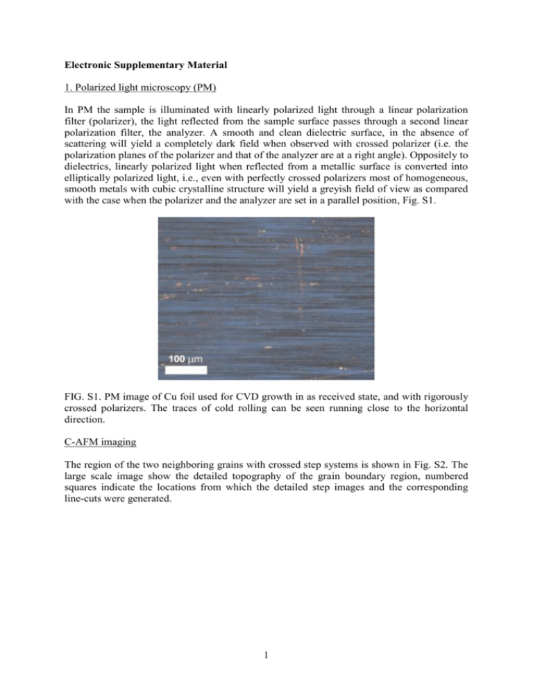
Electronic Supplementary Material 1. Polarized light microscopy (PM) In PM the sample is illuminated with linearly polarized light through a linear polarization filter (polarizer), the light reflected from the sample surface passes through a second linear polarization filter, the analyzer. A smooth and clean dielectric surface, in the absence of scattering will yield a completely dark field when observed with crossed polarizer (i.e. the polarization planes of the polarizer and that of the analyzer are at a right angle). Oppositely to dielectrics, linearly polarized light when reflected from a metallic surface is converted into elliptically polarized light, i.e., even with perfectly crossed polarizers most of homogeneous, smooth metals with cubic crystalline structure will yield a greyish field of view as compared with the case when the polarizer and the analyzer are set in a parallel position, Fig. S1. FIG. S1. PM image of Cu foil used for CVD growth in as received state, and with rigorously crossed polarizers. The traces of cold rolling can be seen running close to the horizontal direction. C-AFM imaging The region of the two neighboring grains with crossed step systems is shown in Fig. S2. The large scale image show the detailed topography of the grain boundary region, numbered squares indicate the locations from which the detailed step images and the corresponding line-cuts were generated. 1 FIG. S2. (top) AFM topography image of the copper grain boundary shown in Fig. 1. (bottom) higher magnification images and line-cuts of the surface step structure on each copper grain. 2 The four lobed individual graphene grain shown in Fig. 2 of the main text was imaged by conductive tip AFM, and SEM, too (Fig. S3). The conductive tip AFM image in agreement with the friction force image clearly shows that the graphene layer is continuous in those regions, where the step structure is missing and where no color is observed in the PM images shown in the main text. FIG. S3. (left) conductive AFM measurement on the graphene flake shown in Fig. 2 (main text). (right) SEM image of the same flake. Spectrogoniometric measurements The spectral data show the relative reflectance of the sample with respect to a reference that is chosen according to the particular conditions of the experiment. As a good external standard was not available, an internal standard the so called “color neutrality” position of the sample was chosen as 100 % reference. In this position the graphene layer covering the steps is in an intermediate position between that corresponding to yellow and violet colors. For the results shown in Fig. 3b and Fig. S4 the sample and the polarizer were kept fix, while the analyzer was rotated. In this way the field of view has a large brightness change, the brightest being when the polarizer and the analyzer are aligned (0° and 180°) and the darkest when they are crossed (90°). In spectral measurements we choose the 0° position as a 100 % reference. 3 FIG. S4. Full set of reflectance curves acquired with sample and polarizer fixed and rotating the analyzer from parallel to fully crossed position towards left(+Δ) and towards right (-Δ). Graphene transferred onto SiO2 To make sure that the coloration is due to the copper step – graphene system as a whole, we have checked the behavior of graphene flakes transferred to a SiO2 substrate with an oxide thickness of 90 nm (Fig. S5). The transfer method is described in detail in an earlier publication [1]. On this substrate the graphene crystallites showed a slightly darker blue color as that of the SiO2/Si, Fig. S4 and did not exhibited any color change under similar conditions as used for the PM investigations described in the main text. FIG. S5. Transferred graphene flakes on SiO2 substrate P. Nemes-Incze, K.J. Yoo, L. Tapasztó, G. Dobrik, J. Lábár, Z.E. Horváth, C. Hwang, and L.P. Biró, Applied Physics Letters 99, 023104-1-023104-3 (2011). 1 4
