Limits on electron quality in suspended graphene
advertisement
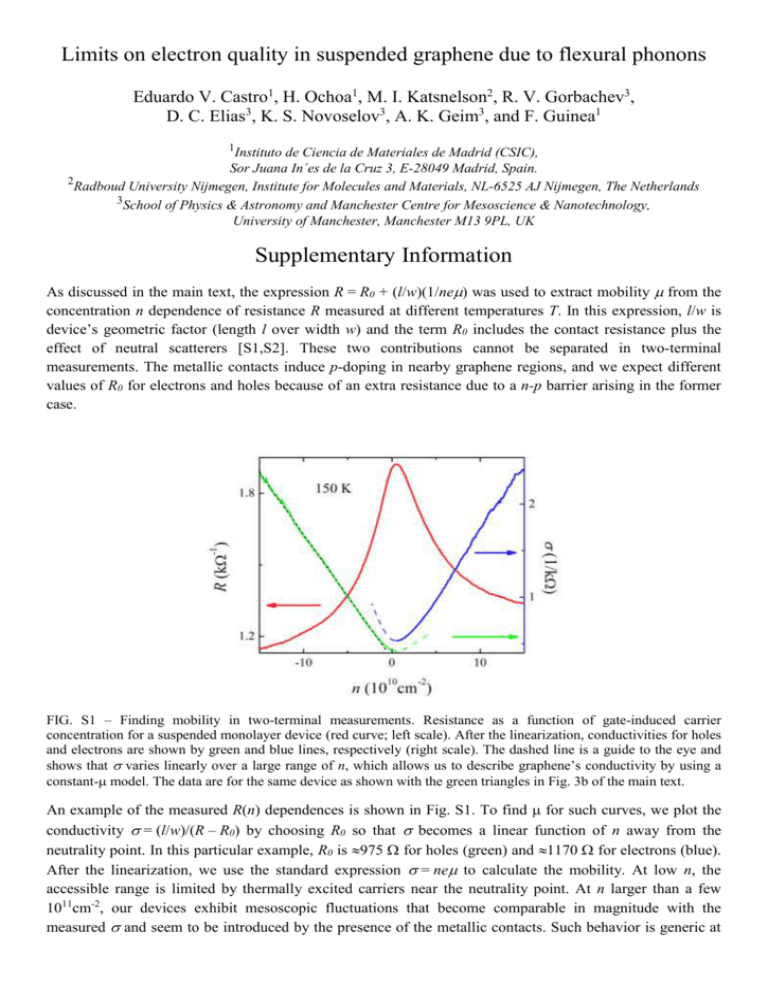
Limits on electron quality in suspended graphene due to flexural phonons Eduardo V. Castro1, H. Ochoa1, M. I. Katsnelson2, R. V. Gorbachev3, D. C. Elias3, K. S. Novoselov3, A. K. Geim3, and F. Guinea1 1 Instituto de Ciencia de Materiales de Madrid (CSIC), Sor Juana In´es de la Cruz 3, E-28049 Madrid, Spain. 2 Radboud University Nijmegen, Institute for Molecules and Materials, NL-6525 AJ Nijmegen, The Netherlands 3 School of Physics & Astronomy and Manchester Centre for Mesoscience & Nanotechnology, University of Manchester, Manchester M13 9PL, UK Supplementary Information As discussed in the main text, the expression R = R0 + (l/w)(1/ne) was used to extract mobility from the concentration n dependence of resistance R measured at different temperatures T. In this expression, l/w is device’s geometric factor (length l over width w) and the term R0 includes the contact resistance plus the effect of neutral scatterers [S1,S2]. These two contributions cannot be separated in two-terminal measurements. The metallic contacts induce p-doping in nearby graphene regions, and we expect different values of R0 for electrons and holes because of an extra resistance due to a n-p barrier arising in the former case. FIG. S1 – Finding mobility in two-terminal measurements. Resistance as a function of gate-induced carrier concentration for a suspended monolayer device (red curve; left scale). After the linearization, conductivities for holes and electrons are shown by green and blue lines, respectively (right scale). The dashed line is a guide to the eye and shows that varies linearly over a large range of n, which allows us to describe graphene’s conductivity by using a constant- model. The data are for the same device as shown with the green triangles in Fig. 3b of the main text. An example of the measured R(n) dependences is shown in Fig. S1. To find for such curves, we plot the conductivity = (l/w)/(R – R0) by choosing R0 so that becomes a linear function of n away from the neutrality point. In this particular example, R0 is 975 for holes (green) and 1170 for electrons (blue). After the linearization, we use the standard expression = ne to calculate the mobility. At low n, the accessible range is limited by thermally excited carriers near the neutrality point. At n larger than a few 1011cm-2, our devices exhibit mesoscopic fluctuations that become comparable in magnitude with the measured and seem to be introduced by the presence of the metallic contacts. Such behavior is generic at T > 100K. At lower T, the accessible range of n is further limited because we reach the ballistic regime [S1], in which the concept of mobility is no longer applicable. For example, at T <20 K, the ballistic regime for one-micron-long devices is typically reached for n > ±1010cm-2. At low T where the thermal smearing of Shubnikov-de Haas (SdH) oscillations is weak, we find that the transport mobility T obtained as described above is in good agreement with quantum mobility Q estimated from the onset of Shubnikov-de Haas oscillations. Similar agreement was previously reported for graphene on oxidized Si wafers with ~1 m2/Vs [S3] and for suspended samples with ~10 m2/Vs [S2]. Our samples exhibit an order of magnitude higher and, therefore, it is essential to crosscheck whether the same relation holds in our case, especially at low T where the range of n allowing the use of the constant T model shrinks significantly. To illustrate this agreement, Fig. S2 shows magnetotransport measurements for one of our devices (the sample is represented by the red squares in Fig. 3b of the main text). One can clearly see that Landau levels start forming at BS ~100 G. By using the standard expression QBS ~1, we roughly estimate the quantum mobility as of about 100 m2/Vs. This value is in agreement with T =105 ±5 m2/Vs which was obtained from the R(n) analysis described above. This extends the previously reached conclusions [S2,S3] (that in graphene T ~Q) to much higher mobilities. FIG S. 2 – Quantum versus transport mobility. Resistance as a function of gate voltage in different magnetic fields; T = 2 K. Shubnikov-de Haas oscillations appear in B ~100G which corresponds to a transport mobility of ~100 m2/Vs. References. S1 - X. Du et al., Nature Nanotech. 3 491 (2008). S2 - K. I. Bolotin et al., Solid State Commun. 146 351 (2008). S3 - M. Monteverde et al., Phys. Rev. Lett. 104, 126801 (2010).
