Template for Electronic Submission to ACS Journals
SUPPLEMENTARY INFORMATION FOR:
Diameter-Controlled and Surface-Modified Sb
2
Se
3
Nanowires and Their Photodetector
Performance
Donghyeuk Choi, Yamujin Jang, Jee Hee Lee, Gyoung Hwa Jeong, Dongmok Whang, Sung Woo
Hwang, Kyung-Sang Cho*, and Sang-Wook Kim* correspondence to: swkim@ajou.ac.kr (S.-W.K.); k-s.cho@samsung.com (K.-S.C.)
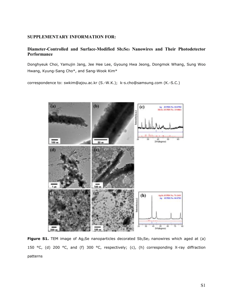
Figure S1. TEM image of Ag
2
Se nanoparticles decorated Sb
2
Se
3
nanowires which aged at (a)
150 °C, (d) 200 °C, and (f) 300 °C, respectively; (c), (h) corresponding X-ray diffraction patterns
S1
Figure S2. SEM images of (a) a bare Sb
2
Se
3
nanowire, and selenium to silver ratio (b) 200/1,
(c) 100/1, and (d) 50/1.
Figure S3. TEM image of width-controlled Ag
2
Se nanoparticles (a), (b) the Ag
2
Se nanoparticles size of 25~30 nm on the Sb
2
Se
3
nanowires diameter of 200-300 nm, (c),(d) the Ag
2
Se nanoparticles size of 10 nm on the Sb
2
Se
3
nanowires diameter of 50 nm.
S2
Figure S4. STEM image of the Ag
2
Se decorated Sb
2
Se
3
nanowires and the EDX-STEM elemental spot analysis of Se, Ag, and Sb elements. O
1
spot on Sb
2
Se
3
nanowires consist of antimony and selenium and O
2
spot on the Ag
2
Se consist of silver and selenium.
Figure S5. The dependence of VB and CB profiles in nanowires as a diameter. The nanowire is fully depleted and band bending is minimal at below the critical diameter (d c
). The recombination barrier increases, thus the photo-carrier lifetime is prolonged at longer nanowire diameter than the critical diameter (d c
).
S3
Figure S6. The energy band diagram near the surface of the Sb
2
Se
3
nanowire before (a) and after Ag
2
Se decoration (b). CB and VB are the conduction band and valence band, respectively.
Surface adsorbed oxygen molecules capture electrons and form depletion layer. After Ag
2
Se decoration, electron flow from Ag
2
Se to nanowire surface, thus depletion at the nanowire surface decreases by charge redistribution.
S4
