Liquid Crystal Polymer (LCP) Substrates and Packages
advertisement
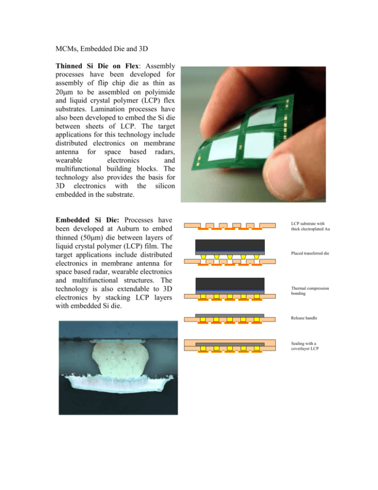
MCMs, Embedded Die and 3D Thinned Si Die on Flex: Assembly processes have been developed for assembly of flip chip die as thin as 20m to be assembled on polyimide and liquid crystal polymer (LCP) flex substrates. Lamination processes have also been developed to embed the Si die between sheets of LCP. The target applications for this technology include distributed electronics on membrane antenna for space based radars, wearable electronics and multifunctional building blocks. The technology also provides the basis for 3D electronics with the silicon embedded in the substrate. Embedded Si Die: Processes have been developed at Auburn to embed thinned (50m) die between layers of liquid crystal polymer (LCP) film. The target applications include distributed electronics in membrane antenna for space based radar, wearable electronics and multifunctional structures. The technology is also extendable to 3D electronics by stacking LCP layers with embedded Si die. LCP substrate with thick electroplated Au Placed transferred die Thermal compression bonding Release handle Sealing with a coverlayer LCP Multichip Modules: Auburn has developed a multilayer Cu/polyimide process on Si, AlN and Si3N4 substrates to fabricate multichip modules. Decoupling capacitors and resistors are also being fabricated as part of the substrate fabrication. The semiconductor die are attached and interconnected to the substrate using wire bonding and flip chip assembly. Additional passive components are surface mount soldered to the substrate. The assembled module is then packaged in a ceramic package and sealed. Die Stacking: Auburn researchers have evaluated materials and demonstrated processes for stacking die in a BGA package. Wire bonding was used to provide the vertical interconnections between the die and the package. Die stacking provides one method of 3D pacakging which is used widely in the cell phone industry.

