srep03070-s1
advertisement
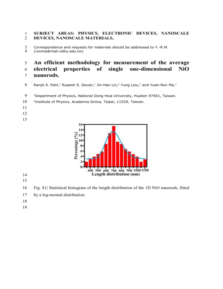
1 2 SUBJECT AREAS: PHYSICS, ELECTRONIC DEVICES, NANOSCALE DEVICES, NANOSCALE MATERIALS, 3 4 Correspondence and requests for materials should be addressed to Y.-R.M. (ronma@mail.ndhu.edu.tw) 5 7 An efficient methodology for measurement of the average electrical properties of single one-dimensional NiO nanorods. 8 Ranjit A. Patil,1 Rupesh S. Devan,1 Jin-Han Lin,2 Yung Liou,2 and Yuan-Ron Ma.1 6 9 10 11 12 13 1 Department of Physics, National Dong Hwa University, Hualien 97401, Taiwan. 2 Institute of Physics, Academia Sinica, Taipei, 11529, Taiwan. 14 15 16 Fig. S1| Statistical histogram of the length distribution of the 1D NiO nanorods, fitted 17 by a log-normal distribution. 18 19 1 2 Fig. S2| TEM images and SAED pattern of a single 1D NiO nanorod (a) Low- 3 magnification TEM image of a single 1D NiO nanorod. The arrow indicates that the 4 nanorod grows along the [200] direction. (b)-(c) high-magnification TEM images 5 showing portions of atomic-resolution lattice planes, taken from the edge regions in 6 the selected areas highlighted in the red and yellow boxes in (a) and (b), respectively. 7 (d) SAED pattern taken from the selected area highlighted in the yellow box, shows a 8 set of symmetric diffraction spots indexed to the [001] zone axis. 9 1 2 3 Fig. S3| IV curves obtained for various 1D NiO nanorod samples and at varying 4 temperatures (a) IV curves obtained for six various 1D NiO nanorod samples. (b) IV 5 curves obtained at temperatures of 90, 130, 170, 300 K. All IV curves are well smooth 6 and get very little fluctuations. 7
