Stephen C - Thilenius
advertisement
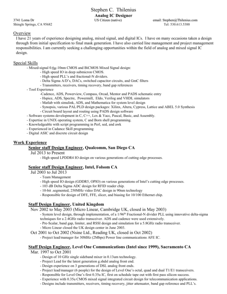
Stephen C. Thilenius Analog IC Designer 3741 Loma Dr Shingle Springs, CA 95682 US Citizen (native) email: Stephen@Thilenius.com Tel: 530.613.5388 Overview I have 21 years of experience designing analog, mixed signal, and digital ICs. I have on many occasions taken a design through from initial specification to final mask generation. I have also carried line management and project management responsibilities. I am currently seeking a challenging opportunities within the field of analog and mixed signal IC design. Special Skills - Mixed-signal 0.6µ-10nm CMOS and BiCMOS Mixed Signal design: - High speed IO in deep submicron CMOS. - High speed PLL’s and fractional-N dividers. - Delta Sigma A/D’s, DACs, switched capacitor circuits, and GmC filters - Transmitters, receivers, timing recovery, band gap references - Tool Experience -Cadence, ADS, Powerview, Compass, Orcad, Mentor and PADS schematic entry - Hspice, ADS, Spectre, Powermill, Eldo, Verilog and VHDL simulators - Matlab with simulink, ADS, and Mathematica for system level design - Synopsis, various PAL/PLD design packages: Xilinx, Altera, Cypress, Lattice and ABEL 5.0 Synthesis - Circuit board layout and routing using PADS design software - Software systems development in C, C++, Lex & Yacc, Pascal, Basic, and Assembly. - Expertise in UNIX operating system, C and Born shell programming. - Knowledgeable with script programming in Perl, sed, and awk - Experienced in Cadance Skill programming - Digital ASIC and discrete circuit design Work Experience Senior staff Design Engineer, Qualcomm, San Diego CA Jul 2013 to Present - High speed LPDDR4 IO design on various generations of cutting edge processes. Senior staff Design Engineer, Intel, Folsom CA Jul 2003 to Jul 2013 - Team Management - High speed IO design (GDDR5, OPIO) on various generations of Intel’s cutting edge processes. - 103 dB Delta Sigma ADC design for RFID reader chip. - 10-bit .segmented, 250MHz video DAC design in 90nm technology - Responsible for design of DFE, FFE, slicer, and biasing for 10/100 Ethernet chip. Staff Design Engineer, United Kingdom Nov 2002 to May 2003 (Micro Linear, Cambridge UK, closed in May 2003) - System level design, through implementation, of a 1/96th Fractional-N divider PLL using innovative delta-sigma techniques for a 2.4GHz radio transceiver. ADS and cadence were used extensively. - Pre-Scalar, band gap, limiter, and RSSI design and simulation for a 5.8GHz radio transceiver. - Micro Linear closed the UK design center in June 2003. Oct 2001 to Oct 2002 (Nsine Ltd., Reading UK, closed in Oct 2002) - Project lead/manager for 30MHz (2Mbps) Power line communications AFE IC. Staff Design Engineer, Level One Communications (Intel since 1999), Sacramento CA Mar. 1997 to Oct 2001 - Design of 10 GHz single sideband mixer in 0.13um technology. - Project Lead for the latest generation g.shdsl analog front end. - Design experience on 3 generations of DSL analog front ends. - Project lead/manager (6 people) for the design of Level One’s octal, quad and dual T1/E1 transceivers. - Responsible for Level One’s first 0.35u IC, first on schedule tape out with first pass silicon success. - Experience with 0.35u CMOS mixed signal integrated circuit design for telecommunication applications. - Designs include transmitters, receivers, timing recovery, jitter attenuator, band gap reference and PLL’s. Design Engineer, Motorola, Tempe AZ Nov. 1995 to Mar. 1997 - Experience with the Smartmos3 BiCMOS Analog integrated circuit design for automotive applications. - Responsible for the redesign of Motorola’s Smartmos3 octal driver. - Principal designer of the UART based physical layer IC working directly with the customer. - Team designer for an ultra low input offset dual opamp. Aug. 1994 to Nov. 1995 - Principal designer of a multiprocessor board for the IO sub-system for the Gemini fault tolerant computer system, including SCSI, Ethernet, and 68020 processors and DRAM controller. - Implementation originally intended for digital ASIC design, however design was cost effectively implemented with FPGA’s. - Expertise in the use of Cadence Concept and Mentor Graphics tools. ASIC Design Engineer, SIS Microelectronics, Longmont CO Jan. 1992 to Jul. 1994 - Gate Array and Cell based ASIC design, layout, and verification. - Expertise in the use of Compass ASIC tools (VLSI), from design conception through physical layout. - Experience with Verilog and AHDL entry using both Synopsis and Compass netlist generation. - Collaborated with customer on DSP audio IC. ECL Digital Design Engineer, Dr. Jon Sauer, Optical Computing Center, Boulder CO Aug. 1991 to Aug. 1993 - Involved in the design of an experimental high speed optical interconnect network. - Designed a complex interface card for the IBM PC using Xilinx FPGA’s to test and operate the new network. - Using Pads Logic and PCB, designed 2 high-speed ECL circuit boards. Consulting Projects, Consultant for various companies in the Boulder Area May 1990 to Aug. 1994 - Design of custom interface cards for the IBM compatible PC. - Borland C/C++ and OWL 2.0 Windows Software Systems Development. - Circuit Board designs and layouts. Education 1990-1991 1987-1990 M.S. Electrical Engineering, University of Colorado, Boulder CO B.S. Electrical Engineering, University of Colorado, Boulder CO Personal I enjoy adventure and travel. I am a native US Citizen Fluent in German
