Supplemental materials - Ge island nucleation and
advertisement
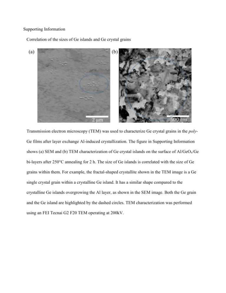
Supporting Information Correlation of the sizes of Ge islands and Ge crystal grains Transmission electron microscopy (TEM) was used to characterize Ge crystal grains in the polyGe films after layer exchange Al-induced crystallization. The figure in Supporting Information shows (a) SEM and (b) TEM characterization of Ge crystal islands on the surface of Al/GeOx/Ge bi-layers after 250°C annealing for 2 h. The size of Ge islands is correlated with the size of Ge grains within them. For example, the fractal-shaped crystallite shown in the TEM image is a Ge single crystal grain within a crystalline Ge island. It has a similar shape compared to the crystalline Ge islands overgrowing the Al layer, as shown in the SEM image. Both the Ge grain and the Ge island are highlighted by the dashed circles. TEM characterization was performed using an FEI Tecnai G2 F20 TEM operating at 200kV.
