L 11 Circuit protection components
advertisement
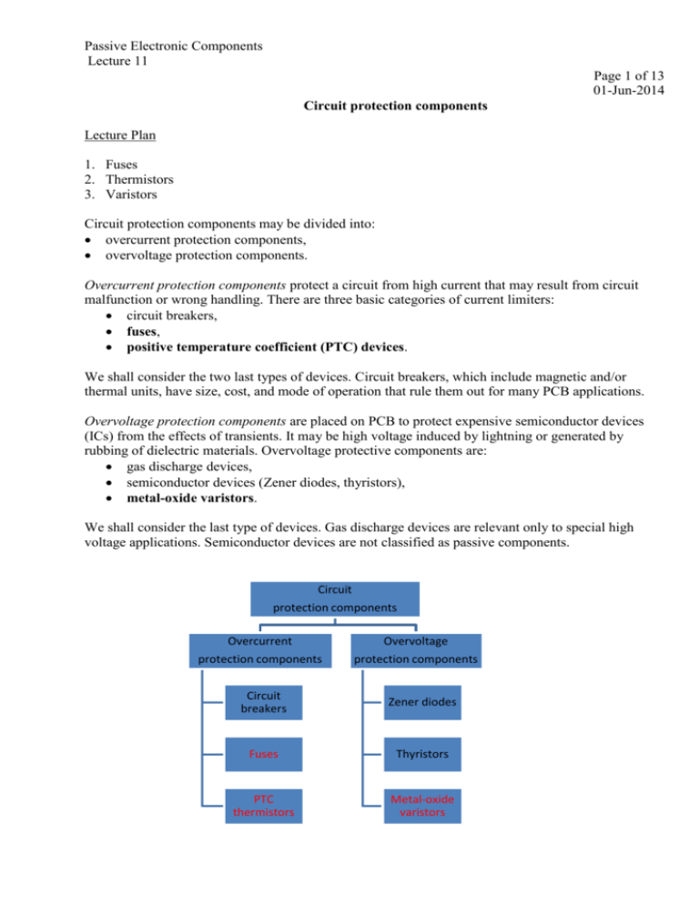
Passive Electronic Components Lecture 11 Page 1 of 13 01-Jun-2014 Circuit protection components Lecture Plan 1. Fuses 2. Thermistors 3. Varistors Circuit protection components may be divided into: overcurrent protection components, overvoltage protection components. Overcurrent protection components protect a circuit from high current that may result from circuit malfunction or wrong handling. There are three basic categories of current limiters: circuit breakers, fuses, positive temperature coefficient (PTC) devices. We shall consider the two last types of devices. Circuit breakers, which include magnetic and/or thermal units, have size, cost, and mode of operation that rule them out for many PCB applications. Overvoltage protection components are placed on PCB to protect expensive semiconductor devices (ICs) from the effects of transients. It may be high voltage induced by lightning or generated by rubbing of dielectric materials. Overvoltage protective components are: gas discharge devices, semiconductor devices (Zener diodes, thyristors), metal-oxide varistors. We shall consider the last type of devices. Gas discharge devices are relevant only to special high voltage applications. Semiconductor devices are not classified as passive components. Circuit protection components Overcurrent Overvoltage protection components protection components Circuit breakers Zener diodes Fuses Thyristors PTC thermistors Metal-oxide varistors Passive Electronic Components Lecture 11 Page 2 of13 1. Fuses. Fuse is a type of sacrificial overcurrent protection device. Its essential component is a metal element that melts when too much current flows across it and interrupts the current. Fuse was patented by Thomas Edison in 1890. Construction and principle of operation. Typical fuse comprises metallic part that is called fusing element. It may be strip, wire, film deposited on ceramics (Fig.1, 2, 3). Fusing element is supposed to be destructed by abnormally high current. In fuses that interrupt high electrical power fusing element is commonly surrounded by sand filler and encapsulated in fire-proof fuse body (Fig.1). In the smallest chip fuses the element is deposited on a chip substrate surface (Fig.3). The element is connected to the fuse terminals. The element configuration, mass, and material are selected to achieve the desired electrical and thermal characteristics. The current passing through the fuse element generates a heat. The heat is dissipated to the ambiance. The higher is thermal resistance between the element and ambiance the less power is needed for fuse activation, the less electrical resistance of fuse is required, the less is voltage drop on the fuse. Notches in the fusing element concentrate heat dissipation in small areas increasing thermal resistance of the fuse. When the current reaches some critical value the element temperature reaches its melting point, melts and fuse opens. The higher is the current the shorter time is needed for element to melt. Such inverse time/current characteristic (Fig.4) is desirable because it meets the property of electronic circuits to carry low level overloads safely for relatively long time and to fail quickly under significant overload. A properly selected fuse can provide effective protection over a broad range of the current. Typically fusing element is made of some elemental metal (copper, tin, etc.). Elemental metals have very high TCR (more than 4103 ppm/K) that results in quick rise of fuse resistance and acceleration of fuse clearing. Blade fuse Fig.1. Blade fuse construction Miniature fuses Cap Element Glass tube Fig.2. Miniature fuse construction Passive Electronic Components Lecture 11 Page 3 of13 Subminiature fuses Chip fuses Terminal Protective coat Film element Fig.3. Chip fuse construction Ceramic substrate The main parameters of a fuse. Current rating I n , A – nominal value of current. It is maximal safe current that fuse can pass through for unlimited time at particular ambient temperature. Commonly a fuse is derated 25% regarding normal load. For example 10 A fuse is typically used for load of 7.5 A. Fuse actuation is a thermal process therefore maximal safe current depends on ambient temperature: the lower is a temperature the higher is a maximal safe current. According to recommendations of manufacturer the fuse has to be in addition derated or uprated depending on the circuit temperature. Voltage rating U n , V – maximal voltage that can be applied to the terminals of actuated (burnt out) fuse. Breaking capacity I max , A – maximum current that a fuse can safely interrupt at rated voltage (and any voltage below U n ). Time/current characteristics – graphically specified functional relationship between current value and clearing time (interval of time between the instant of current starting and the instant of current interruption). According to relationship between clearing time and current a fuse may be fast acting or slow blow (time delay). Passive Electronic Components Lecture 11 Page 4 of13 Particular fuse standard specifies some points in this curve. For example IEC 60127-4 standard specifies time/current characteristics as the following: Current 1.25 I n Time 1 hour 2 In < 2 min 10 I n t <0.001 s (FF) 0.001 t 0.01 (F) 0.01< t 0.1 (T) 0.1< t 1.0 (TT) Designations: FF - very quick acting, F - quick acting, T - time-lag, TT - long time-lag. Fig.4. Typical time/current characteristics of fuse. 2. Thermistors. Thermistors NTC PTC (ceramic) Linear (silicone, metal, thickfilm) Switching (ceramic, polymer) A thermistor is a thermally sensitive resistor. There are two basic types of thermistors: negative temperature coefficient (NTC) thermistors, positive temperature coefficient (PTC) thermistors. Passive Electronic Components Lecture 11 Page 5 of13 PTC thermistors. PTC thermistors may be linear or non-linear (switching). Only switching PTC thermistors may be directly used as circuit protection devices. Nevertheless, we shall consider both types of PTC thermistors. Linear PTC Thermistors. Thermally sensitive silicon thermistors, sometimes referred to as “silistors”. These devices exhibit a fairly uniform positive temperature coefficient (about +0.77% /K) through most of their operational range, but can also exhibit a negative temperature coefficient region at temperatures in excess of 150°C. These devices are most often used for temperature compensation of silicon semiconducting devices in the range of -60°C…+150°C. Pure metal (Platinum, Nickel) thermistors. They may be manufactured using thin-film or wirewound technology. Nickel thin-film thermistors have TCR about +0.41% /K at +25°C. Platinum thin-film thermistors have TCR about +0.38% /K in 0…+100°C temperature range. Thick-film thermistors have TCR range about +0.10… +0.36% /K depending on resistance values. Switching PTC Thermistors. Commercial switching PTC thermistors are ceramic or polymer. At some critical temperature these devices begin to exhibit high positive temperature coefficient of resistance and therefore a large increase in resistance. The resistance change can be as much as several orders of magnitude within a temperature span of a few degrees. Resistance – Temperature Characteristics of PTC Thermistors: Silistor and Switching Type Ceramic switching type PTC thermistors. Ceramic PTC devices have ability: to operate in high-voltage circuits, to return to normal operating resistance with great accuracy. Passive Electronic Components Lecture 11 Page 6 of13 They exhibit a very small negative temperature coefficient until the device reaches a critical temperature, that is referred to as its Curie (switch, transition) temperature. When the critical temperature is exceeded resistance of the thermistor rises several orders of magnitude. The raw material is doped polycrystalline ceramic on the basis of barium titanate. Generally, ceramic is known as a good insulating material with a high resistance. A low resistance is achieved by doping the ceramic with materials of a higher valency than that of the crystal lattice. The material structure is composed of many individual crystallites (as shown in the picture). At the edge of these monocrystallites, the potential barriers are formed. They prevent free electrons from diffusing into adjacent areas. The result is high resistance of the grain boundaries. However, this effect is neutralized at low temperatures. In a certain range of temperature above the Curie temperature, the resistance of the PTC thermistor rises exponentially. Mixtures of barium carbonate, titanium oxide and other materials whose composition produces the desired electrical and thermal characteristics are ground, mixed and compressed into disks, washers, rods, slabs or tubular shapes depending on the application. These blank parts are then sintered, preferably at temperatures below 1400 °C. Afterwards, they are provided with terminals and finally coated or encased. Ceramic PTC devices’ size, which is inherently larger than that of equivalent miniature fuses, can be a problem in products with high component density and limited space. Ceramic PTC materials also have a high thermal mass, which means that their reaction time to a moderate overcurrent may be longer than sensitive components’ time to damage. Moreover, ceramic PTC materials have an inherently high normal resistance. This can preclude their use in low-voltage circuits in which the voltage drop across the resistance can interfere with the load’s operation. Polymer switching type PTC thermistors. A more recent development in PTC technology overcomes ceramic devices’ size and reaction-time problems. Polymer PTCs are made of a slice of plastic with carbon grains embedded in it. When the device is cool, the carbon grains are in close contact with each other, forming a conductive path through the device. As the device heats up, the plastic expands and the grains move further apart, raising the total resistance of the device. Passive Electronic Components Lecture 11 Page 7 of13 In general, polymer devices suit to the circuits operating at less than 60V with normal currents of less than 15A. The relationship between electrical and thermal parameters of a thermistor at steady state condition follows from equality of electrical power dissipated in thermistor and thermal power escaped from thermistor to ambiance. T Ta U2 , R T Rth U – voltage applied to thermistor, T – thermistor temperature, Ta – ambient temperature, Rth – thermal resistance between thermistor and ambiance, R(T) – electrical resistance of thermistor at temperature T. Using of PTC thermistor for protection from overcurrent resulted from load resistance decrease. V0 Overload operation Non-resetting operation Automatically resetting operation RL V0 The above figure illustrates operating states of a PTC fuse. There are: V-I curve (brown); three load lines corresponding to three resistance values of the load L (RL2<RL1<RL). V V0 I RL ; I V0 V . RL Red load line corresponds to overload state with the lowest load resistance RL. In this state current is limited by high resistance of thermistor. Rated operation corresponding to blue line is nonresetting automatically after overload ending. Rated operation corresponding to green line automatically resets after overload ending. Using of PTC thermistor for protection from overcurrent resulted from voltage rise At that RL2=RL1 . When voltage V0 rises from value V01 to value V02 the circuit current drops down and corresponds to point E in the below graph. Passive Electronic Components Lecture 11 Page 8 of13 V V02 V01 Using of PTC thermistor for temperature protection Position of current-voltage curve of the thermistor after temperature rise is indicated by red line in the below graph. V V0 Common applications of PTC thermistors are: Motor start. Fluorescent lamp start. Degaussing. Power semiconductors protection Self-regulated heaters (in thermostats). Resettable fuses. Liquid level sensors. Passive Electronic Components Lecture 11 Page 9 of13 Compact fluorescent lamp circuit Liquid level sensors Transformer protection Power semiconductors protection NTC thermistors are resistors with a high negative temperature coefficient. They are much more commonly used than PTC thermistors. The first NTC thermistor was discovered in 1833 by Michael Faraday, who reported on the semiconducting behavior of silver sulfide. Commercial production of thermistors began only in the 1930s. NTC thermistors are the most sensitive of all the temperature sensing elements and have a rapid response time. Interchangeability with tolerances 0.1…0.2 °C is another important feature. NTC thermistors are hard and rugged sensors. They are able to handle mechanical and thermal shocks better than any other temperature measuring device. The listed properties make the thermistors ideal for precise temperature sensing and compensation. The resistance of a thermistor as a function of temperature is approximated by expression 1 1 R (T ) R0 exp B , T T0 where B - a material constant (B value), K; T - thermistor temperature, K; Ro - the resistance of the thermistor at temperature To. Usually To = 25C = 298K. Ro ranges from some Ohms to several megaohms. The B value is a function of the material composition. Its range is about 2500K … 5000K. Thermistors with B values 3000K … 4000K are frequently used for measurement purposes. Manufacturing of NTC thermistors. The raw materials are different oxides of metals such as manganese, iron, cobalt, nickel, copper and zinc. The oxides are milled to a powdery mass, mixed with a plastic binder and then compressed into the desired shape. Standard shapes are disk and wafer. The blanks are then sintered at high temperatures (1000 … 1400 °C) to produce the Passive Electronic Components Lecture 11 Page 10 of13 polycrystalline thermistor body. Disks are provided with terminals by baking a silver paste onto the flat surfaces and attaching the leads. Depending on the application, the thermistors are coated or additionally incorporated in different kinds of housing. Finally the thermistors are subjected to a special ageing process to ensure high stability of the electrical values. (Otherwise the NTC resistance would possibly change even at room temperature due to solid-state reactions in the polycrystalline material). SMD NTC thermistors (chip thermistors) may be produced using ceramic multilayer technology or may be diced from a piece of bulk ceramics. Multilayer structure allows lower resistance at high B constant. Parameters of NTC thermistors. Resistance Temperature Coefficient The resistance temperature coefficient () of a thermistor is the rate of change of the resistance per 1C temperature change. It is expressed in percent change per 1C (or 1K) and is given by: 1 dR B 100% 2 100% . R dT T Typical values of resistance temperature coefficient are in -2…-5 %/C range. Dissipation Constant Dissipation constant (or dissipation factor) of a thermistor th is the amount of power needed to raise the temperature of the thermistor due to self-heating by 1K when thermistor is mounted on standard glass-epoxy board (1.2mm thick). Dissipation constant is measured in [W/K]. th P , T TA where P – power consumed by thermistor, W; T –thermistor temperature, K; TA –ambient temperature, K. It should be noticed that th is reciprocal value of thermal resistance Rt T TA P between the component and ambiance. Self heating of a thermistor results in non-linear current-voltage dependence: Passive Electronic Components Lecture 11 Page 11 of13 Power Rating The power rating Prated is the maximum continuous power that thermistor can withstand based on maximum permissible temperature rise. Self-heating will limit the power rating to the following equation: Prated Tmax TA th , where T A is ambient temperature +25°C, Tmax is maximum permissible temperature of thermistor. 3. Varistors. Varistors (Variable Resistors or VDRs - Voltage Dependent Resistors) are two-terminal components with a symmetrical V/I characteristic curve. Resistance of varistor decreases sharply when applied voltage exceeds the certain threshold. Varistor is connected in parallel with the electronic device or circuit that is to be guarded. It forms a low-resistance shunt when voltage increases and thus prevents the overvoltage. The current-voltage dependence of varistors may be approximately characterized by the formula I KV , where may be interpreted as a measure for the “steepness” of the V-I curve. In metal oxide varistors > 30. This makes V-I curve of varistors similar to that of symmetrical Zener diodes. But exceptional current handling capability, less than 25 ns (in multilayer SMD varistors less than 0.5 ns) response times, and low price make them an almost perfect protective device when compared to diodes. Varistor: circuit diagram symbol and typical V/I characteristic curve Microstructure and conduction mechanism Sintering zinc oxide together with other metal oxide additives under specific conditions produces a polycrystalline ceramic whose resistance exhibits a pronounced dependence on voltage. This phenomenon is called the varistor effect. Passive Electronic Components Lecture 11 Page 12 of13 The above figure shows the conduction mechanism in a varistor element in simplified form. The zinc oxide grains themselves are highly conductive, while the intergranular boundary formed of other oxides is highly resistive. Only at those points where zinc oxide grains meet each other does “microvaristors” are formed that are comparable to symmetrical Zener diodes with protection level approximately 3.5 V. The electrical behavior of the metal oxide varistor results from the number of microvaristors connected in series or in parallel. This implies that the electrical properties are controlled by the physical dimensions of the varistor. Twice the ceramic thickness produces twice the protection level because then twice as many microvaristors are arranged in series. Twice the area produces twice the current handling capability because double number of current paths is arranged in parallel. Twice the volume produces almost twice the energy absorption capability because there are twice as many absorbers in the form of zinc oxide grains. The series and parallel connection of the individual microvaristors in the sintered body also explains its high electrical load capacity compared to semiconductors. While the power in semiconductor devices is dissipated almost entirely in the thin p-n junction area, in a varistor it is distributed over all the microvaristors, i. e. uniformly throughout the component’s volume. This permits high absorption of energy and thus exceptionally high surge current handling capability. Parameters of varistor Max. operating voltage (RMS AC and DC), V Varistor voltage @ 1 mA, V Max. clamping voltage @ 1 A, V Max. average power dissipation, W Max. surge current (8/20 µs), A Max. energy absorption (ESD), J Description It may be exceeded by transients only It has no particular physical significance but is often used as a practical standard reference. It characterizes protection level of varistor. Varistors: leaded (left), surface mount chip and chip array (right) Passive Electronic Components Lecture 11 Page 13 of13 Equivalent circuit of varistor Application examples.
