Basic Electrical Engineering
advertisement
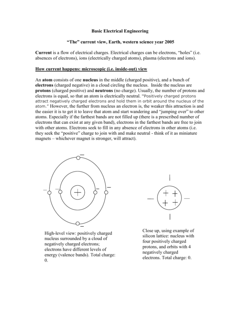
Basic Electrical Engineering “The” current view, Earth, western science year 2005 Current is a flow of electrical charges. Electrical charges can be electrons, “holes” (i.e. absences of electrons), ions (electrically charged atoms), plasma (electrons and ions). How current happens: microscopic (i.e. inside-out) view An atom consists of one nucleus in the middle (charged positive), and a bunch of electrons (charged negative) in a cloud circling the nucleus. Inside the nucleus are protons (charged positive) and neutrons (no charge). Usually, the number of protons and electrons is equal, so that an atom is electrically neutral. “Positively charged protons attract negatively charged electrons and hold them in orbit around the nucleus of the atom.” However, the further from nucleus an electron is, the weaker this attraction is and the easier it is to get it to leave that atom and start wandering and “jumping over” to other atoms. Especially if the farthest bands are not filled up (there is a prescribed number of electrons that can exist at any given band), electrons in the farthest bands are free to join with other atoms. Electrons seek to fill in any absence of electrons in other atoms (i.e. they seek the “positive” charge to join with and make neutral - think of it as miniature magnets – whichever magnet is stronger, will attract). High-level view: positively charged nucleus surrounded by a cloud of negatively charged electrons; electrons have different levels of energy (valence bands). Total charge: 0. Close up, using example of silicon lattice: nucleus with four positively charged protons, and orbits with 4 negatively charged electrons. Total charge: 0. Conductors are materials which have a lot of free electrons, therefore the free electrons can be easily moved and thus produce current. All metals are good conductors. Electrical wires are made out of conductors. Semiconductors are materials which are insulators below room temperature but conduct at room temperature or when excited in some other way (optically, etc.) Diodes and transistors are made out of semiconductors. Insulators are materials which do not conduct electrical current because it is too hard to pull any electrons out of completely filled valence bands and get them moving. Plastic is an insulator. Capacitor filling is made of out insulator. Electrical cables (made out of conductors) and shielded with insulators. How current happens: macroscopic (i.e. outside-in) view: Current is analogous through water flowing. It needs a path, and it always seeks the path of least resistance. Current can continue flowing only if the path (called electric circuit) is closed, i.e. the path forms a loop, and there is something that keeps on moving the charges along. A power supply is a device that coaxes charges to keep on moving, i.e. it adds enough energy to atoms to make the electrons leave the atoms and move. Voltage is the difference between electric potential of two points. The reference is totally arbitrary, it is sufficient that one point has more positive charge than the other. The point with more positive charge is called higher potential. Electrons want to move from low potential to high potential. As electrons are moving in one direction, they leave “empty spaces,” i.e. positive charges, behind them, so we can say that the positive charges move in the opposite direction than electrons. Think of electrons as cars on the parking lot, or people sitting in a row. If there is one empty space, then the closest car will move into it; then the next car will move in the newly created empty space, etc. So, cars are moving in one direction, and empty spaces are moving in the opposite direction. Conventional current flow is a convention that states that the current flows in the direction of positive charges. Inside a battery, the + side is on high potential, the – side is on the low potential. Electrons cannot keep on moving from – to + inside the battery, because it is not a closed loop. So, if we connect the battery into a circuit, e.g. a resistor, then current can flow. It will flow from the battery -, through the circuit, and then through the battery + into the battery -. (The battery operates on chemical reaction and is physically constructed so that electrons will find it easier to go from the battery – through the circuit, instead of from the battery – through the battery and to the battery +). So, battery does not produce any electrons, it just “pushes them along.” It is the same electrons moving around. e e- shows the flow of negative charges, i.e. electrons: from battery – to battery +, and then through battery - E e+ e+ shows the flow of positive charges, i.e. absence of electrons: from battery + to battery -, and then through battery Semiconductors, p-n junction, Diodes and Transistors Semiconductors are materials which are insulators below room temperature but conduct at room temperature. Semiconductors’ properties can be enhanced by doping. Doping is the process by which impurities are introduced into a semiconductor material. An impurity is a material which is suitable for creating excess electrons or excess holes in the semiconductor, so that the semiconductor can conduct well. If the impurities have more electrons than the doped semiconductor, then the doping results in an n-type semiconductor. If the impurities have less electrons, then a p-type semiconductor is obtained. For example, silicon is a semiconductor that has 4 protons and 4 electrons, and is usually doped with phosphorus or arsenic (which have 5 electrons) to obtain an n-type semiconductor, or with boron (which has 3 electrons) to obtain a p-type semiconductor. hole Example of p-type semiconductor: silicon doped with boron extra electron Example of n-type semiconductor: silicon doped with arsenic or phosphorus In summary: 1. n-type semiconductors have an excess of electrons (they are doped with negative charges, i.e. extra electrons are added). For n-type semiconductors, the majority carriers are electrons, and minority carriers are holes. 2. p-type semiconductors have a lack of electrons, i.e. an excess of “holes” where those electrons should have been, i.e. some electrons are missing. For p-type semiconductors, the majority carriers are holes, and minority carriers are electrons. A p-n junction is obtained when a p-type semiconductor is joined with an n-type semiconductor. A diode is an implementation of the p-n junction where the p-type semiconductor is the anode, and the n-type is the cathode. A transistor is a p-n-p junction or an n-p-n junction. It can be made as a bipolar junction transistor (BJT) or a field effect transistor (FET), which can be MOSFET, JFET, etc. The kind of transistor is obtained by physically arranging p and n portions on the chip in certain ways. http://en.wikipedia.org/wiki/Bipolar_junction_transistor “A p-n junction may be created by doping adjacent regions of a semiconductor with ptype and n-type dopants. If a positive bias voltage is placed on the p-type side, the dominant positive carriers (holes) are pushed toward the junction. At the same time, the dominant negative carriers (electrons) in the n-type material are attracted toward the junction. Since there is an abundance of carriers at the junction, current can flow through the junction from a power supply, such as a battery. However, if the bias is reversed, the holes and electrons are pulled away from the junction, leaving a region of relatively nonconducting silicon which inhibits current flow. The p-n junction is the basis of an electronic device called a diode, which allows electric current to flow in only one direction. Similarly, a third region can be doped n-type or p-type to form a three-terminal device, such as the bipolar junction transistor (which can be either p-n-p or n-p-n).” [Wikipedia] p n e- e+ Forward biased p-n junction: the diode conducts current due to majority carriers http://www.tpub.com/content/ neets/14179/css/14179_32.ht m p e+ e- Reverse biased p-n junction: the diode does not fully conduct current; but there is a tiny reverse current due to minority carriers http://www.tpub.com/content/neets/ 14179/css/14179_33.htm n Schematic symbol for a diode (with p and n parts labeled) p n p C E C e+ B B p-n-p bipolar junction transistor (BJT) : microscopic view and schematic symbol http://www.infodotinc.com/neets/book7/25b.htm E n p n IC C E C IB e+ B B IE E IE = IB + IC n-p-n bipolar junction transistor (BJT) : microscopic view and schematic symbol http://www.infodotinc.com/neets/book7/25a.htm http://www.tpub.com/content/neets/14179/css/14179_70.htm Joke of the day: A hydrogen atom and a helium atom go into a bar. The hydrogen atom is clearly upset and moans, "I've lost my electron, my only electron." The concerned helium atom says, "Just calm down now ... are you sure you've lost it?" The hydrogen atom replies, "Yes, I'm positive!" (Later, a neutron walks in to the same bar. He sits down and says to the bar tender, "Hey, how much for a beer?" The bar tender looks at him and says, "For you, no charge!") Quiz: why is this joke funny? http://en.wikipedia.org/wiki/Semiconductor http://www.tpub.com/content/neets/14179/ http://en.wikipedia.org/wiki/Electrical_conduction http://www.dl.ket.org/physics/companion/ThePC/compan/Current/ http://www.infodotinc.com/neets/book7/25b.htm Transistors A common way to use an n-p-n BJT is to connect it in the common emitter mode. Use Kirchoff’s laws to calculate the currents. Input voltage is considered to be VBE, and output voltage can be taken as VE or VCE, depending on what we want. Input current is IB, and output current is either IC or IE. A transistor can work either as an amplifier or as a switch. Amplifiers are used mostly for electronics, and switches are the basis for gates used to implement Boolean algebra. Used for switching: shaded yellow (cutoff mode) and shaded red (saturation mode). Used for amplification: no shade (forward active mode). http://www.mitedu.freeserve.co.uk/Design/bjtsw.htm IC C IB B IE E Always: IE = IB + IC If amplifier: IC = βIB VBE = 0.7V If in saturation mode: VCE = 0.7V IC = Isaturation If you don’t have transistor characteristics, then you have to determine on your own if the transistor is saturated or not. Calculate IC as minimum between Isaturation and βIB 1. Transistor as amplifier: When the input voltage is low enough, then the transistor’s p-n junctions behave as we discussed already (BE is forward biased, CB is reverse biased), and the entire transistor behaves as an amplifier. It is said that the transistor works in the active mode. In the active mode, BE junction is a forward biased diode, and thus VBE = 0.7 Volts (some people take it as low as 0.5V or 0.6V) when the transistor is ON. IB should be very small (usually μA). Usually, β=100, so IC is on the order of mA. Example: run a motor using a logic gate as the input. http://www2.ics.hawaii.edu/%7Epagerg/331/7 http://www2.ics.hawaii.edu/%7Epagerg/331/9 2. Transistor as switch: When the input voltage VBE is too high and thus produces high input current, BE overpowers BC, i.e. BE is higher than CB. BE is forward biased and because it overpowered BC, BC is forward biased too. The transistor works in the saturation mode. In the saturation mode, VCE is almost 0, usually VCE = 0.2V. When VBE is low, the transistor cannot work because the BE diode is not on, therefore the entire transistor is off, i.e. not working. When the transistor is off, it means that it acts as an open circuit, which means that the output voltage VCE is high, i.e. almost straight from the power supply. If we take the output voltage to be VCE and run the transistor between cutoff mode and saturation mode, then the transistor behaves as an inverter. When VBE is high, the transistor is in saturation mode and so VCE is low; when VBE is low, the transistor is in cutoff mode and so VCE is high. Example: turn a light on and off. http://www.mitedu.freeserve.co.uk/Design/bjtsw.htm

