Schottky Junctions & Semiconductor Physics Assignment
advertisement
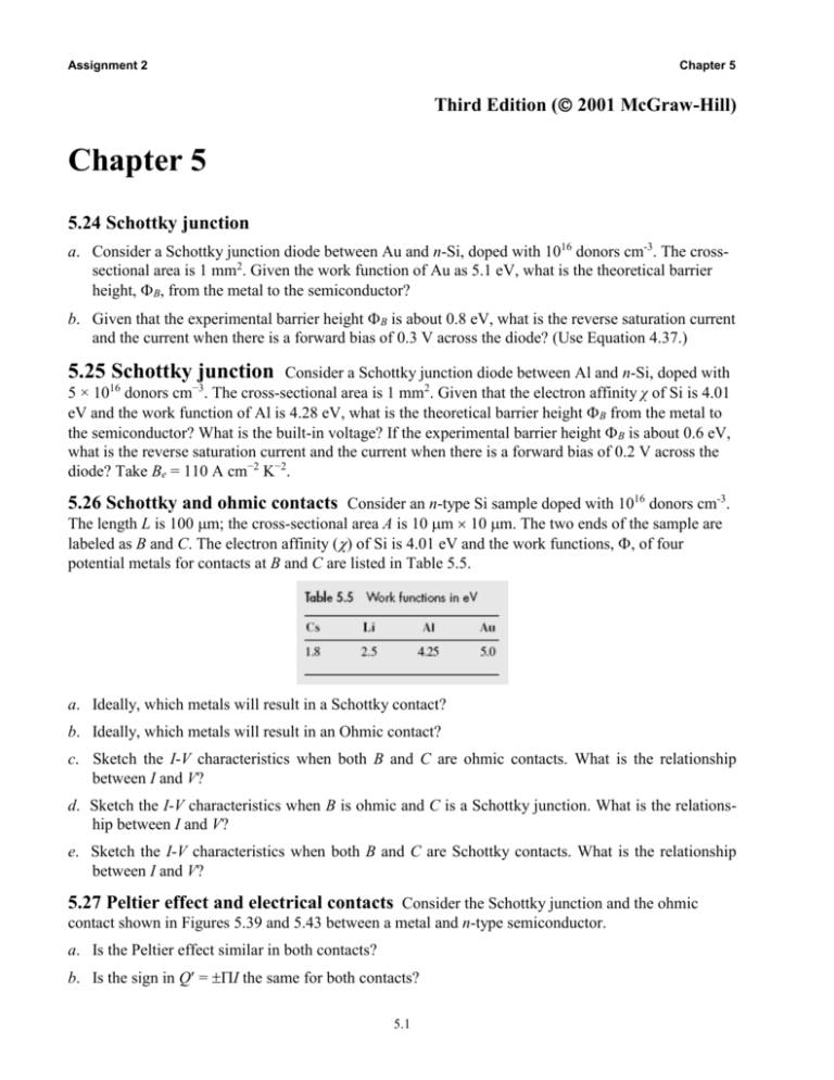
Assignment 2 Chapter 5 Third Edition ( 2001 McGraw-Hill) Chapter 5 5.24 Schottky junction a. Consider a Schottky junction diode between Au and n-Si, doped with 1016 donors cm-3. The crosssectional area is 1 mm2. Given the work function of Au as 5.1 eV, what is the theoretical barrier height, B, from the metal to the semiconductor? b. Given that the experimental barrier height B is about 0.8 eV, what is the reverse saturation current and the current when there is a forward bias of 0.3 V across the diode? (Use Equation 4.37.) 5.25 Schottky junction Consider a Schottky junction diode between Al and n-Si, doped with 5 × 10¹⁶ donors cm−3. The cross-sectional area is 1 mm2. Given that the electron affinity χ of Si is 4.01 eV and the work function of Al is 4.28 eV, what is the theoretical barrier height B from the metal to the semiconductor? What is the built-in voltage? If the experimental barrier height B is about 0.6 eV, what is the reverse saturation current and the current when there is a forward bias of 0.2 V across the diode? Take Be = 110 A cm−2 K−2. 5.26 Schottky and ohmic contacts Consider an n-type Si sample doped with 1016 donors cm-3. The length L is 100 m; the cross-sectional area A is 10 m 10 m. The two ends of the sample are labeled as B and C. The electron affinity () of Si is 4.01 eV and the work functions, , of four potential metals for contacts at B and C are listed in Table 5.5. a. Ideally, which metals will result in a Schottky contact? b. Ideally, which metals will result in an Ohmic contact? c. Sketch the I-V characteristics when both B and C are ohmic contacts. What is the relationship between I and V? d. Sketch the I-V characteristics when B is ohmic and C is a Schottky junction. What is the relationship between I and V? e. Sketch the I-V characteristics when both B and C are Schottky contacts. What is the relationship between I and V? 5.27 Peltier effect and electrical contacts Consider the Schottky junction and the ohmic contact shown in Figures 5.39 and 5.43 between a metal and n-type semiconductor. a. Is the Peltier effect similar in both contacts? b. Is the sign in Q = I the same for both contacts? 5.1 Assignment 2 Chapter 5 c. Which junction would you choose for a thermoelectric cooler? Give reasons. *5.28 Peltier coolers and figure of merit (FOM) Consider the thermoelectric effect shown in Figure 5.45 in which a semiconductor has two contacts at its ends and is conducting an electric current I. We assume that the cold junction is at a temperature Tc and the hot junction is at Th and that there is a temperature difference of T = ThTc between the two ends of the semiconductor. The current I flowing through the cold junction absorbs Peltier heat at a rate Q'P, given by QP= I [5.95] where is the Peltier coefficient for the junction between the metal and semiconductor. The current I flowing through the semiconductor generates heat due to the Joule heating of the semiconductor. The rate of Joule heat generated through the bulk of the semiconductor is L QJ I 2 A [5.96] We assume that half of this heat flows to the cold junction. In addition there is heat flow from the hot to the cold junction through the semiconductor, given by the thermal conduction equation A QTC T L [5.97] The net rate of heat absorption (cooling rate) at the cold junction is then Qnet cool = QP 1/2QJ QTC [5.98] By substituting from Equations 5.95 to 5.97 into Equation 5.98, obtain the net cooling rate in terms of the current I. Then by differentiating Qnet cool with respect to current, show that maximum cooling is obtained when the current is A I m L [5.99] and the maximum cooling is cool Qmax A 1 2 T L 2 [5.100] Under steady state operating conditions, the temperature difference, T, reaches a steady-state value and the net cooling rate at the junction is then zero (T is constant). From Equation 6 show that the maximum temperature difference achievable is 5.2 Assignment 2 Chapter 5 Tmax 1 2 2 [5.101] The quantity 2/k is defined as the figure of merit (FOM) for the semiconductor as it determines the maximum T achievable. The same expression also applies to metals, though we will not derive it here. Use Table 5.6 to determine the FOM for various materials listed therein and discuss the significance of your calculations. Would you recommend a thermoelectric cooler based on a metal-tometal junction? 5.3
