Ben- Gurion University of the Negev Materials Engineering Name of
advertisement
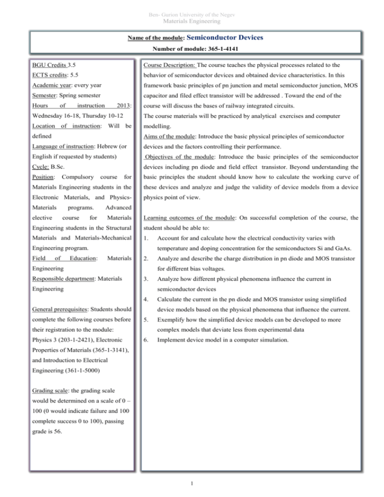
Ben- Gurion University of the Negev Materials Engineering Name of the module: Semiconductor Devices Number of module: 365-1-4141 BGU Credits 3.5 Course Description: The course teaches the physical processes related to the ECTS credits: 5.5 behavior of semiconductor devices and obtained device characteristics. In this Academic year: every year framework basic principles of pn junction and metal semiconductor junction, MOS Semester: Spring semester capacitor and filed effect transistor will be addressed . Toward the end of the Hours of instruction 2013: course will discuss the bases of railway integrated circuits. Wednesday 16-18, Thursday 10-12 The course materials will be practiced by analytical exercises and computer Location of instruction: Will be modelling. defined Aims of the module: Introduce the basic physical principles of semiconductor Language of instruction: Hebrew (or devices and the factors controlling their performance. English if requested by students) Objectives of the module: Introduce the basic principles of the semiconductor Cycle: B.Sc. devices including pn diode and field effect transistor. Beyond understanding the Position: Compulsory for basic principles the student should know how to calculate the working curve of Materials Engineering students in the these devices and analyze and judge the validity of device models from a device Electronic Materials, and Physics- physics point of view. Materials elective programs. course for course Advanced Materials Learning outcomes of the module: On successful completion of the course, the Engineering students in the Structural student should be able to: Materials and Materials-Mechanical 1. Engineering program. Field of Education: Account for and calculate how the electrical conductivity varies with temperature and doping concentration for the semiconductors Si and GaAs. Materials 2. Engineering Responsible department: Materials for different bias voltages. 3. Engineering General prerequisites: Students should Calculate the current in the pn diode and MOS transistor using simplified device models based on the physical phenomena that influence the current. 5. their registration to the module: Physics 3 (203-1-2421), Electronic Analyze how different physical phenomena influence the current in semiconductor devices 4. complete the following courses before Analyze and describe the charge distribution in pn diode and MOS transistor Exemplify how the simplified device models can be developed to more complex models that deviate less from experimental data 6. Implement device model in a computer simulation. Properties of Materials (365-1-3141), and Introduction to Electrical Engineering (361-1-5000) Grading scale: the grading scale would be determined on a scale of 0 – 100 (0 would indicate failure and 100 complete success 0 to 100), passing grade is 56. 1 Ben- Gurion University of the Negev Materials Engineering Lecturer: Professor Nurit Ashkenasy Attendance regulation: Attendance in class is not mandatory Contact details: Building 59, room Teaching arrangement and method of instruction: Lectures and exercises. 11 Office phone: 08-6472494 Assessment: Email: nurita@bgu.ac.il Office hours: 1. Final Exam 65% Lecturer: 2. Midterm exam 20% Sunday 15:00-16:00, 3. Exercises 5% Thursday 15:00-16:00 4. Computer exercises 10% TA: will be announced. 100% Module evaluation: at the end of the semester the students will evaluate Work and assignments: The students are expected to follow classes and lecture the in order to draw notes, and supplement by reading in the text –book of the course, as well as conclusions, and for the university's complementary literature. The students will receive exercises every 2 or 3 weeks, internal needs. and in addition 3-4 computer exercises during the semester. Their solutions will be module, examined and will be used to access their marks in the course as described above. Confirmation: the syllabus was confirmed by the faculty academic Time required for individual work: in addition to attendance in class, the students advisory committee to be valid on are expected to do their assignment and individual work: at least 3 hours per week. 2012-2013. Module Content\ schedule and outlines: Last update: January 24, 2013 1. Introduction: energy bands of semiconductors, density of states, carrier distribution functions, carrier densities (3h). 2. 3. 4. 5. 6. 7. 8. Carrier transport: mobility, carrier drift and diffusion, velocity saturation, (2h). Carrier recombination and generation: quasi-Fermi levels, the continuity equation and the diffusion equation (2h). p-n junction at equilibrium: band diagram and built in potential, the depletion approximation (3h). The p-n diode current: the ideal diode current, deviation from ideality, reverse bias breakdown, the junction capacitance (7h). Metal-Semiconductor junctions: structure and principle of operation, thermal equilibrium, forward and reverse bias, metal semiconductor contacts (4h). Metal-Oxide-Silicon capacitors: structure and principle of operation, MOS capacitor analysis (6h) MOS Field Effect Transistors: structure and principle of operation, MOSFET analysis, threshold voltage, advanced MOSFET issues, CMOS, MOSFET memory (12h) Required reading: "Solid State Electronic Devices” by B. G. Streetman and S. K. Banerjee. Additional literature: "Physics of Semiconductor Devices" S.M. Sze and K. Ng. Kwok "מוליכים למחצה ושימושיהם" זאב בורשטיין * Learning material will be available to the students on the module's website (high-learn)/ library/ electronic documents available to BGU students. 2
