Separated Carbon Nanotube Macroelectronics for
advertisement
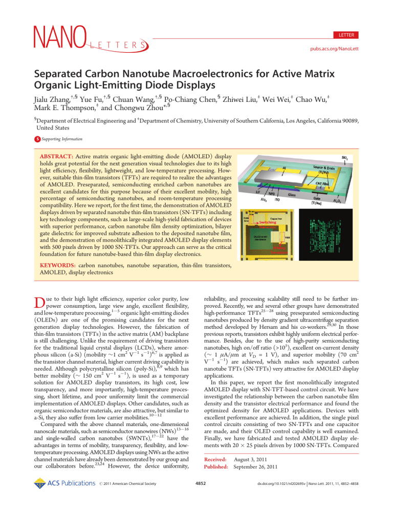
LETTER pubs.acs.org/NanoLett Separated Carbon Nanotube Macroelectronics for Active Matrix Organic Light-Emitting Diode Displays Jialu Zhang,†,§ Yue Fu,†,§ Chuan Wang,†,§ Po-Chiang Chen,§ Zhiwei Liu,‡ Wei Wei,‡ Chao Wu,‡ Mark E. Thompson,‡ and Chongwu Zhou*,§ § Department of Electrical Engineering and ‡Department of Chemistry, University of Southern California, Los Angeles, California 90089, United States bS Supporting Information ABSTRACT: Active matrix organic light-emitting diode (AMOLED) display holds great potential for the next generation visual technologies due to its high light efficiency, flexibility, lightweight, and low-temperature processing. However, suitable thin-film transistors (TFTs) are required to realize the advantages of AMOLED. Preseparated, semiconducting enriched carbon nanotubes are excellent candidates for this purpose because of their excellent mobility, high percentage of semiconducting nanotubes, and room-temperature processing compatibility. Here we report, for the first time, the demonstration of AMOLED displays driven by separated nanotube thin-film transistors (SN-TFTs) including key technology components, such as large-scale high-yield fabrication of devices with superior performance, carbon nanotube film density optimization, bilayer gate dielectric for improved substrate adhesion to the deposited nanotube film, and the demonstration of monolithically integrated AMOLED display elements with 500 pixels driven by 1000 SN-TFTs. Our approach can serve as the critical foundation for future nanotube-based thin-film display electronics. KEYWORDS: carbon nanotubes, nanotube separation, thin-film transistors, AMOLED, display electronics D ue to their high light efficiency, superior color purity, low power consumption, large view angle, excellent flexibility, and low-temperature processing,15 organic light-emitting diodes (OLEDs) are one of the promising candidates for the next generation display technologies. However, the fabrication of thin-film transistors (TFTs) in the active matrix (AM) backplane is still challenging. Unlike the requirement of driving transistors for the traditional liquid crystal displays (LCDs), where amorphous silicon (a-Si) (mobility ∼1 cm2 V1 s1)6,7 is applied as the transistor channel material, higher current driving capability is needed. Although polycrystalline silicon (poly-Si),8,9 which has better mobility (∼ 150 cm2 V1 s1), is used as a temporary solution for AMOLED display transistors, its high cost, low transparency, and more importantly, high-temperature processing, short lifetime, and poor uniformity limit the commercial implementation of AMOLED displays. Other candidates, such as organic semiconductor materials, are also attractive, but similar to a-Si, they also suffer from low carrier mobilities.1012 Compared with the above channel materials, one-dimensional nanoscale materials, such as semiconductor nanowires (NWs)1316 and single-walled carbon nanotubes (SWNTs),1722 have the advantages in terms of mobility, transparency, flexibility, and lowtemperature processing. AMOLED displays using NWs as the active channel materials have already been demonstrated by our group and our collaborators before.23,24 However, the device uniformity, r 2011 American Chemical Society reliability, and processing scalability still need to be further improved. Recently, we and several other groups have demonstrated high-performance TFTs2528 using preseparated semiconducting nanotubes produced by density gradient ultracentrifuge separation method developed by Hersam and his co-workers.29,30 In those previous reports, transistors exhibit highly uniform electrical performance. Besides, due to the use of high-purity semiconducting nanotubes, high on/off ratio (>105), excellent on-current density (∼ 1 μA/μm at VD = 1 V), and superior mobility (70 cm2 V1 s1) are achieved, which makes such separated carbon nanotube TFTs (SN-TFTs) very attractive for AMOLED display applications. In this paper, we report the first monolithically integrated AMOLED display with SN-TFT-based control circuit. We have investigated the relationship between the carbon nanotube film density and the transistor electrical performance and found the optimized density for AMOLED applications. Devices with excellent performance are achieved. In addition, the single pixel control circuits consisting of two SN-TFTs and one capacitor are made, and their OLED control capability is well examined. Finally, we have fabricated and tested AMOLED display elements with 20 25 pixels driven by 1000 SN-TFTs. Compared Received: August 3, 2011 Published: September 26, 2011 4852 dx.doi.org/10.1021/nl202695v | Nano Lett. 2011, 11, 4852–4858 Nano Letters LETTER Figure 1. Structure of AMOLED circuit and layout. (a) Schematic diagram for the circuit of AMOLED. Each pixel contains one switching transistor, one driving transistor, one charge storage capacitor, and an OLED. (b) Top view for the layout of a single pixel AMOLED with an area of 500 500 μm2. (c) Cross-sectional view for the structure of the AMOLED pixel consisting of a glass substrate, patterned Ti/Au gate electrode, Al2O3 gate dielectric, separated CNT thin film for the active channel, Ti/Pd source and drain contacts, integrated OLED (ITO/NPD/Alq3/LiF/Al), and a SiO2 passivation layer. with conventional platforms, our SN-TFT platform shows significant advantages, such as low-temperature processing compatibility, scalability, reproducibility, and device performance, and suggests a practical and realistic approach for carbon nanotubebased AMOLED display applications. Figure 1a illustrates the schematic diagram of the AMOLED circuit with the red box showing the circuit structure within one pixel. Each pixel contains one switching transistor (Ts), one driving transistor (Td), one charge storage capacitor (Cs), and one OLED.5 The switching transistor, controlled by the signal from the scan line, is employed to select one specific row of pixels in an AMOLED display element by passing the signal from data line through the channel of the switching transistor to the gate of the driving transistor. The driving transistor further controls the output light intensity of the OLED pixel by modulating the current flowing through OLED. For the line-by-line scanning technique presented in the display technology nowadays, the capacitor Cs is used to store and stabilize the voltage obtained from the data line during one scanning period, which is crucial for dynamic displays. Based on the circuit diagram, the corresponding layout of one pixel is shown in Figure 1b and c (top and cross-sectional views, respectively). The single pixel layout has a total area of 500 500 μm2 with OLED area of 200 200 μm2 and is designed to be fabricated on glass substrate with patterned Ti/Au (5 Å/40 nm) gate electrode, Al2O3 (40 nm) gate dielectric, separated nanotube thin film for the active channel, Ti/Pd (5 Å/50 nm) source and drain contacts, integrated green OLED, and a 200 nm SiO2 passivation layer. The total fabrication consists of 7 photo masks and 15 fabrication steps. In order to control the OLED intensity, the transistors in the control circuits need to have high current on/off ratio and excellent current drive capability. Shorter channel length and higher nanotube channel network density would lead to high on-current density, which is needed for OLED display applications. However, it will also create more metallic nanotube pass in the channel, which will negatively affect the transistor current on/off ratio. Therefore, for the OLED control purpose, optimized device geometry and channel nanotube network density are very important. A 98% semiconducting carbon nanotube solution (from Nanointegris, Inc.; batch no. S08665) was used, as suggested by previous work from our group,25 to produce a uniform, separated nanotube thin-film on aminopropyltriethoxy silane 4853 dx.doi.org/10.1021/nl202695v |Nano Lett. 2011, 11, 4852–4858 Nano Letters LETTER Figure 2. Carbon nanotube TFT performance as a function of nanotube density. (ac) FE-SEM images of separated CNT thin films with different densities obtained by tuning the ratio of APTES and IPA used in the surface functionalization process. (d) Relationship between nanotube film density and APTES: IPA ratio. (e, f) Channel length dependence of device on/off ratio (e) and normalized on current (f) for transistors fabricated on nanotube films using different APTES: IPA ratios. (blue trace for APTES: IPA = 1:100, red trace for APTES: IPA = 1:10, and green trace for APTES: IPA = 1:1). (APTES) functionalized Si/SiO2 surface by solution-based deposition technique.26,31 After treating the silicon wafer with a APTES solution and rinsing, the wafer is soaked in the preseparated solution of semiconducting nanotubes for 30 min to give a thin film of carbon nanotubes on the silicon surface. The nanotube network density can be controlled by tuning the concentration of APTES in isopropanol alcohol (IPA) solution used for SiO2 surface treatment, before nanotube deposition. Three different conditions are studied (APTES:IPA = 1:1, 1:10, and 1:100), and the field-emission scanning electron microscopy (FE-SEM) images of the resulting nanotube thin-film are exhibited in Figure 2ac. From the images, one can find that the nanotube density varies significantly when different volume ratios of APTES and IPA are used. From Figure 2d, one can see that the sample with APTES:IPA ratio of 1:1 has low nanotube network density (4 tubes/μm2), and the uniformity of the thin-film is poor. For the sample with APTES:IPA ratio of 1:10, a highly uniform film is obtained with a density of 45 tubes/μm2. Nevertheless, if the solution is further diluted to APTES:IPA = 1:100, the resulting film density decreases to 36 tubes/μm2. When APTES is not applied to the silicon wafer, nanotubes show very low levels of coverage (<0.5 tubes/μm2) under the same conditions.26 The relationship between nanotube film density and APTES:IPA ratio can be explained as follows: The APTES coats the SiO2 surface, forming an amine-terminated monolayer, which captures the nanotubes in solution, binding them to the substrate to form a uniform thin film. When the APTES concentration is very high, instead of a uniform monolayer, multiple layers of APTES molecules are stacked onto the SiO2 surface, leading to an uneven amine surface and thus a low density nanotube film. As the APTES concentration in IPA is diluted, a uniform monolayer APTES molecules is formed, which results in a highly uniform nanotube film with excellent density. However, when the APTES solution is diluted even further, the APTES monolayer may have defects and vacancies, so the amine surface and nanotube film density will decrease again. Atomic force microscope (AFM) images of the SiO2 surface functionalized with different concentration of APTES solution can be found in Supporting Information, S1. Overall, by tuning the concentration of APTES in IPA solution, separated nanotube thin film with different densities can be achieved. Subsequently, electrical performance of the nanotube network with different density is investigated. The 100 transistors with different channel geometry were fabricated on each sample with different nanotube density, and the channel length dependence of device on/off ratio and normalized on current are shown in Figure 2e and f. From these two plots, one can find that due to the benefit of high-purity semiconducting nanotube, all the devices with channel lengths larger than 20 μm have on/off ratios higher than 104, and transistors made with nanotube film deposited using an APTES:IPA ratio of 1:10, which gives the highest nanotube density, also offer the best current driving capability (0.5 μA/μm at VD = 1 V for 20 μm channel length devices). Based on the electrical performance, APTES:IPA ratio of 1:10 and device geometry of L = 20 μm, W = 100 μm were chosen as the optimized conditions for the transistors used in the AMOLED control circuits. Figure 3 shows the structure and electrical characteristics of the nanotube transistors used in the AMOLED. For the sake of two transistors control circuit, individual back-gated device structure was chosen as shown in Figure 3a, where 5 Å Ti and 40 nm Au are patterned as the back gate, and 40 nm Al2O3 is deposited by atomic layer deposition (ALD) as the gate dielectric. Due to the poor adhesion between Al2O3 and APTES molecules, we have found that the deposited nanotube thin film on Al2O3 surface peels off during the ensuing fabrication steps (Supporting Information, S2). In order to improve the adhesion, a thin layer of SiO2 (5 nm) was deposited on top of the Al2O3 layer using electron beam evaporator to form a bilayer gate dielectric. With 4854 dx.doi.org/10.1021/nl202695v |Nano Lett. 2011, 11, 4852–4858 Nano Letters LETTER Figure 3. Electrical properties of transistors used in the AMOLED circuit. (a) Schematic diagram of the back-gated transistor built on separated nanotube thin film with Ti/Au (5 Å/40 nm) back gate, Ti/Pd (5 Å/50 nm) contact electrodes, and the Al2O3/SiO2 bilayer gate dielectric (40 nm/5 nm). (b) FE-SEM image showing the channel of a back-gated SN-TFT with 20 μm channel length. (c) Transfer (IDVG) characteristics (red, linear scale; green, log scale) and gmVG characteristics (blue) of a typical SN-TFT (L = 20 μm, W = 100 μm) with VD = 1 V. (d) Output (IDVD) characteristics of the same device with VG varying from 5 to 5 V in 1 V steps. the help of the evaporated SiO2 layer, uniform nanotube thin film was achieved as shown in Figure 3b. After the separated nanotube thin-film deposition, Ti/Pd (5 Å/50 nm) was applied on top of the channel network to form ohmic source and drain contacts. Finally, the nanotubes outside the channel region were etched away by photolithography and oxygen plasma. Electrical properties of a typical transistor are characterized and plotted in Figure 3c, which contain the transfer (IDVG) characteristics (red curve for linear scale and green curve for log scale) and gmVG characteristics (blue) measured with VD = 1 V. The on current at VD = 1 V and VG = 5 V is 82.9 μA, corresponding to a current density of 0.829 μA/μm. The on/off ratio exceeds 104, and the peak transconductance is 25.5 μS. Based on the transconductance, the device mobility is extracted to be 31.65 cm2 V1 s1. We note that the parallel plate model is used to estimate the gate capacitance when calculating the device mobility due to the complexity of the bilayer gate dielectric structure. If we take the electrostatic coupling between nanotubes into consideration, the gate capacitance will be smaller, and therefore, the real mobility can be larger than the value listed here.32 In addition, the output (IDVD) characteristics of the same device are also measured with VG varying from 5 to 5 V in 1 V steps as shown in Figure 3d, which indicates nice field-effect operation and ohmic contacts. Following the single transistor analysis, the AMOLED pixel control circuits were fabricated and studied. Figure 4a displays the optical microscope image of the fabricated single pixel circuit before OLED integration, which contains two SN-TFTs, one capacitor, and one indiumtin oxide (ITO) electrode for further OLED integration. To operate the driving transistor, 5 V is applied to the scan line to turn on the switching transistor. Transfer (IDDVDATA) characteristics are plotted in Figure 4b and c in linear and logarithm scales, respectively. The various curves in Figure 4b correspond to various values of the supply voltage VDD (0.21 V with 0.2 V steps), which was connected to the source of the driving transistor as shown in the inset schematic diagram in Figure 4c. From the transfer characteristics in logarithm scale, one can find that the two-transistor circuit exhibits excellent on/off ratio (higher than 106), which results from the optimized channel geometry and film density as well as the high semiconducting nanotube purity. This on/off ratio is crucial in order to guarantee that the control circuits can fully turn off the OLED pixels. Beside the on/off ratio, the current drive capability of the circuit is also important for AMOLED displays, which is examined by the output (IDDVDD) characteristics shown in Figure 4d. To keep VGS value of the driving transistor constant, source of the driving transistor is grounded, while the drain terminal (VDD) is swept from 0 V to 7 V, and different curves were obtained with VDATA changing from 5 to 5 V with 1 V steps. From this figure, one can clearly find that current flow through the driving transistor will saturate under high VDD, and with the optimized semiconducting nanotube density, 50 μA is achieved when VDD = 3 V, VDATA = 5 V, and VSCAN = 5 V, which offers high enough current density to drive OLED pixels with the designed area (200 200 μm2). To further understand the behavior of the circuit controlled AMOLED, an OLED was connected to and controlled by a typical single pixel control circuit using wire bonding. Standard 4-4 0 -bis[N-(1-naphthyl)-N-phenyl-amino]biphenyl (NPD)/ Alq3 OLED (2 2 mm2) with multilayered configuration is 4855 dx.doi.org/10.1021/nl202695v |Nano Lett. 2011, 11, 4852–4858 Nano Letters LETTER Figure 4. Characteristics of the two-transistor single-pixel circuit. (a) Optical microscope image of the single pixel circuit with two SN-TFTs, one capacitor, and the ITO electrode for OLED integration. Scale bar is 100 μm. (b, c) Transfer (IDDVDATA) characteristics of the single pixel circuit measured while VSCAN = 5 V in linear scale (VDD = 10.2 V with 0.2 V steps) and logarithm scale (VDD = 1 V), respectively. Inset: schematic diagram of the single pixel circuit. (d) Output (IDDVDD) characteristics measured at VSCAN = 5 V with different VDATA (5 to 5 V with 1 V steps). employed in this study given as ITO/NPD [40 nm]/tris(8hydroxyquinoline) aluminum (Alq3) [40 nm]/LiF [1 nm]/aluminum (Al) [100 nm], whose transfer characteristics are shown in the Supporting Information S3. Organic and metal films were deposited from resistively heated boats under ultrahigh vacuum (UHV) conditions, as reported previously.33 The schematic of the OLED control circuit is shown in the inset of Figure 5a, where the drain of the driving transistor is connected to an external OLED and a negative voltage (VDD) was applied to the cathode of the OLED. The current flow through the OLED (IOLED) was measured by sweeping the VDD while also changing input voltage VDATA, as plotted in Figure 5a. VSCAN is kept to be 5 V to keep the switching transistor on, and the family of curves correspond to various values of VDATA from 5 to 5 V in 1 V steps. The figure illustrates that if VDATA is sufficiently negative, OLED will be turned on when the supply voltage is higher than the threshold voltage of the OLED (about 3 V), and the current flow through OLED will increase as VDATA decreases. Therefore, the light intensity of the OLED can be modulated by VDATA, which is directly revealed in Figure 5b where current and output light intensity versus VDATA characteristics are plotted with a fixed VDD of 8 V, as shown in the inset schematic. From this figure, one can find that when sweeping VDATA from 5 to 5 V, the current through OLED changes from 71 μA to 3.7 nA, and the output light intensity also varies from 5.3 106 to about 8 1012 W/cm2, which exceeds 5 orders of magnitude difference, and the significant change in the light intensity can be visually seen in Figure 5c. The optical photographs represent the OLED under various VDATA voltages of 5, 3, 1, 1, 3, and 5 V, respectively, and demonstrate that the external OLED can be fully turned on and turned off by changing the voltage of VDATA. Based on the discussion above, we went one step forward to fabricate a monolithically integrated AMOLED display element. First, an array of AMOLED control circuit (1 1.25 cm2) with 20 25 pixels driven by 1000 SN-TFTs was fabricated using the same layout design as discussed previously. The pixel size was 200 200 μm2. After preparing the control circuits, 200 nm SiO2 was deposited by electron beam evaporator as a passivation layer, leaving only the prepatterned ITO electrode open for OLED integration. Finally, green OLEDs with the same multilayer structure and thickness (ITO/NPD/Alq3/LiF/Al) as used for the single pixel circuit study were deposited by thermal evaporation onto ITO electrodes. Optical image of a completed AMOLED substrate, which contains 7 AMOLED elements (20 25 pixels each) is shown in Figure 5d. Figure 5e is a photograph showing all the pixels on one integrated AMOLED element, which are turned on when VDATA = 5 V, VSCAN = 5 V, and VDD = 8 V are applied for all the pixels. In this figure, 348 out of 500 pixels are turned on, corresponding to a yield of 70%, which is acceptable for the demonstration purpose in the present laboratory-scale experiments. It is worth noting that many of the failed pixels are due to the top SiO2 surface roughness, which leads to short circuits during OLED evaporation and can be improved by using a better passivation technique. To the best 4856 dx.doi.org/10.1021/nl202695v |Nano Lett. 2011, 11, 4852–4858 Nano Letters LETTER Figure 5. AMOLED display characteristics. (a) Characteristics of the OLED controlled by single pixel circuit, where the current flow through the OLED (IOLED) is measured by sweeping the VDD. The family of curves corresponds to values of VDATA from 5 to 5 V in 1 V steps. (b) Plot of the current through the OLED (IOLED) (red line) and OLED light intensity (green line) versus VDATA with VDD = 8 V. (c) Photographs showing that under different VDATA, the two-transistor single pixel circuit can turn on and off the OLED. (d) Optical image of an AMOLED substrate containing 7 AMOLED elements, each with 20 25 pixels. (e) Photograph showing the pixels on an integrated AMOLED, which are turned on when VDATA = 5 V, VSCAN = 5 V, and VDD = 8 V are applied for the pixels. of our knowledge, this is the first demonstration of AMOLED display driven solely by SN-TFT circuits. In summary, we have demonstrated the great potential of using SN-TFTs for high-performance display electronics. By tuning the concentration of APTES in IPA solution during the surface functionalization step, an optimized separated nanotube thin-film density of 45 tubes/μm is achieved when 1:10 volume ratio between APTES and IPA is used. Based on the optimized nanotube density and device geometry, individual back-gated transistors with superior on/off ratio (>104) and excellent current driving capability (∼0.8 μA/μm) have been fabricated with 20 μm channel length and 100 μm channel width. In addition, the electrical properties and OLED control capability of the single pixel AMOLED control circuit are well examined and analyzed, and the modulation in the output light intensity exceeds 105. Moreover, a monolithically integrated AMOLED display element with 500 pixels and 1000 transistors has been further demonstrated. Our work represents a significant advance in separated nanotube-based macroelectronics and might pave the way of using separated carbon nanotubes for future display applications. ’ ASSOCIATED CONTENT bS Supporting Information. AFM image of the APTEScoated SiO2 surface (S1), separated nanotube thin-film on Al2O3 and Al2O3/SiO2 film (S2), and two terminal measurement of the OLED (S3). This material is available free of charge via the Internet at http://pubs.acs.org. ’ AUTHOR INFORMATION Corresponding Author *E-mail: chongwuz@usc.edu. Author Contributions † These authors contributed equally. ’ ACKNOWLEDGMENT We acknowledge financial support from the National Science Foundation (CCF-0702204) and the Defense Threat Reduction 4857 dx.doi.org/10.1021/nl202695v |Nano Lett. 2011, 11, 4852–4858 Nano Letters Agency (HDTRA1-10-1-0015). We thank Professor Mark Hersam of Northwestern University and Mr. Elliott Garlock and Dr. Nathan Yoder of Nanointegris for valuable discussions. LETTER (32) Cao, Q.; Xia, M.; Kocabas, C.; Shim, M.; Rogers, J. A.; Rotkin, S. V. Appl. Phys. Lett. 2007, 90, 023516–10235163. (33) Wei, W.; Djurovich, P.; Thompson, M. Chem. Mater. 2010, 22 (5), 1724–1731. ’ REFERENCES (1) Forrest, S.; Burrows, P; Thompson, M. Laser Focus World 1995, 31, 99–101, no. 2. (2) Sheats, J; Antoniadis, H; Hueschen, M; Leonard, W; Miller, J; Moon, R; Roitman, D; Stocking, A. Science 1996, 273, 884–888. (3) Tang, C. Dig. Tech. Pap. - Soc. Inf. Disp. Int. Symp. 1996, 27, 181–184. (4) Burrows, P; Forrest, S; Thompson, M. Curr. Opin. Solid State Mater. Sci. 1997, 2, 236–243. (5) Gu, G; Forrest, S. IEEE J. Sel. Top. Quantum Electron. 1998, 4, 83. (6) Snell, A. J.; Mackenzie, K. D.; Spear, W. E.; LeComber, P. G.; Hughes, A. J. Application of Amorphous Silicon Field Effect Transistors in Addressable Liquid Crystal Display Panels. Appl. Phys. A: Mater. Sci. Process. 1981, 24, 357–362. (7) Powell, M. IEEE Trans. Electron Devices 1989, 36, 2753. (8) Ucjikoga, S. MRS Bull. 2002, 27, 881–886. (9) Chang, C; Wu, Y. S. IEEE Electron Device Lett. 2009, 30, 1176. (10) Gelinck, G. H.; Edzer, H.; Huitema, A.; van Veenendaal, E.; Cantatore, E.; Schrijnemakers, L.; van der Putten, J. B. P. H.; Geuns, T. C. T.; Beenhakkers, M.; Giesbers, J. B.; Hiusman, B.-H.; Meijer, E. J.; Benito, E. M.; Touwslager, F. J.; Marsman, A. W.; van Rens, B. J. E.; de Leeuw, D. M. Nat. Mater. 2004, 3, 106–110. (11) Klauk, H.; Halik, M.; Zschieschang, U.; Eder, F.; Rohde, D.; Schmid, G.; Dehm, C. IEEE Trans. Electron Devices 2005, 52, 618–622. (12) Sekitani, T.; Zschieschang, U.; Klauk, H.; Someya, T. Nat. Mater. 2010, 9, 1015–1022. (13) McAlpine, M. C.; Friedman, R. S.; Jin, S.; Lin, K.-H.; Wang, W. U.; Lieber, C. M. Nano Lett. 2003, 3, 1531–1535. (14) Chen, J.; Konenkamp, R. Appl. Phys. Lett. 2003, 82, 4782–4784. (15) Lei, B.; Li, C.; Zhang, D.; Zhou, Q.; Shung, K.; Zhou, C. Appl. Phys. Lett. 2004, 84, 4553–4555. (16) Ju, S. Y.; Facchetti, A.; Xuan, Y.; Liu, J.; Ishikawa, F.; Ye, P. D.; Zhou, C. W.; Marks, T. J.; Janes, D. B. Nat. Nanotechnol. 2007, 2, 378–384. (17) Bockrath, M.; Cobden, D.; McEuen, P.; Chopra, N.; Zettl, A.; Thess, A.; Smalley, R. Science 1997, 275, 1922–1925. (18) Wildoer, J.; Venema, L.; Rinzler, A.; Smalley, R.; Dekker, C. Nature 1998, 391, 59–62. (19) Odom, T.; Huang, J.; Kim, P.; Lieber, C. Nature 1998, 391, 62–64. (20) Ryu, K.; Badmaev, A.; Wang, C.; Lin, A.; Patil, N.; Gomez, L.; Kumar, A.; Mitra, S.; Wong, H.-S. P.; Zhou, C. Nano Lett. 2009, 9, 189–197. (21) Ishikawa, F.; Chang, H.; Ryu, K.; Chen, P.; Badmaev, A.; De Arco Gomez, L.; Shen, G.; Zhou, C. ACS Nano 2009, 3, 73–79. (22) McCarthy, M. A.; Liu1, B.; Donoghue1, E. P.; Kravchenko, I.; Kim, D. Y.; F. So, F.; Rinzler1, A. G. Science 2011, 332, 570–573. (23) Ju, S.; Li, J.; Liu, J.; Chen, P. C.; Ha, Y.; Ishikawa, F.; Chang, H.; Zhou, C.; Faccheti, A.; Janes, D. B.; Marks, T. J. Nano Lett. 2008, 8, 997–1004. (24) Chen, P.; Shen, G.; Chen, H.; Ha, Y.; Wu, C.; Sukcharoenchoke, S.; Fu, Y.; Liu, J.; Facchetti, A.; Marks, T. J. ACS Nano 2009, 3, 3383–3390. (25) Engel, M.; Small, J. P.; Steiner, M.; Freitag, M.; Green, A. A.; Hersam, M. C.; Avouris, P. ACS Nano 2008, 2, 2445–2452. (26) Wang, C.; Zhang, J; Ryu, K.; Badmaev, A.; Gomez, L.; Zhou, C. Nano Lett. 2009, 9, 4285–4291. (27) Wang, C.; Zhang, J.; Zhou, C. ACS Nano 2010, 4, 7123–7132. (28) Zhang, J.; Wang, C.; Fu, Y.; Che, Y.; Zhou, C. ACS Nano 2011, 5, 3284–3292. (29) Arnold, M. S.; Green, A. A.; Hulvat, J. F.; Stupp, S. I.; Hersam, M. C. Nat. Nanotechnol. 2006, 1, 60–65. (30) Arnold, M. S.; Stupp, S. I.; Hersam, M. C. Nano Lett. 2005, 5, 713–718. (31) LeMieux, M. C.; Roberts, M.; Barman, S.; Jin, Y. W.; Kim, J. M.; Bao, Z. Science 2008, 321, 101–104. 4858 dx.doi.org/10.1021/nl202695v |Nano Lett. 2011, 11, 4852–4858


