Comprehensive Portfolio from the Leader in PCI Express Solutions
Integrated DeviceTechnology
CLOCKS AND TIMING
|
INTERFACE AND CONNECTIVITY
|
MEMORY AND LOGIC
|
POWER MANAGEMENT
|
RF PRODUCTS
PCI Express® Timing Solutions
25 MHz
•
•
•
•
•
x
M
N
ZDB
ZDB
2 - 8 O/P + REF
2 In
2 - 19 O/P
1 / 4 O/P
FOB
Eliminate up to 32 resistors
Save up to 55 mm2 of area*
As small as 6.25 mm2
85 and 100 system support
SSC generation
•
•
•
•
•
•
•
•
•
•
Operating
Voltage
Zout ( )
9FGU0241/9FGV0241/9FGL0241/51/P1
9FGV0242
9FGU = 1.5 V
xx41 = 100
Spread
Spectrum
Generation
Resistors
Saved
Area
Saved*
(mm2)
Package
Area (mm2)
Package
Type
Typ. Idd
(mA)
Yes
8
14
16
VFQFPN-24
28
No
8
14
6.25
VFQFPN-16
17
PCIe
Outputs
Ref
Output
2
2
Typ. Gen 3
Jitter w/SSC
(ps rms)
4
Yes
16
27
25
VFQFPN-32
32
6
Yes
24
41
25
VFQFPN-40
39
• Extensive Portfolio
8
Yes
32
55
36
VFQFPN-48
46
0.3 - 0.4
• Up to 64 lane and 24 port devices
PCIe
Outputs
PLL/ZDB
Mode
Resistors
Saved
Area
Saved*
(mm2)
Package
Area (mm2)
Package
Type
Typ. Idd
(mA)
PCIe Gen123 Clock Buffers
Typ. Gen 3
Jitter w/SSC
(ps rms)
9DBU0241/9DBV0241
2
Yes
8
14
16
VFQFPN-24
16
0.5
9DBU0441/9DBV0441
4
Yes
16
27
25
VFQFPN-32
31
0.5
4
No
8
14
16
VFQFPN-20
40
<0.2 additive
9DBU0541/9DBV0541
9DBU = 1.5 V
9DBU0641/9DBV0641
9DBV = 1.8 V
xx41 = 100
5
No
20
34
25
VFQFPN-32
25
<0.1 additive
6
Yes
24
41
25
VFQFPN-40
41
0.5
7
No
28
48
25
VFQFPN-40
34
<0.1 additive
9DBU0841/9DBV0841
8
Yes
32
55
36
VFQFPN-48
46
0.5
9DBU0941/9DBV0941
9
No
36
62
36
VFQFPN-48
44
<0.1 additive
9DBU0741/9DBV0741
xx51 = 85
xxP1 = Prog
Yes
PCIe Gen1/2/3 + QPI Clock Buffers
Part Number
Operating
Voltage
Zout ( )
9ZXL0651
9ZXL1231/1251
9ZXL = 3.3 V
9ZXL1530/50
xx30/31=33
xx50/51=85
9ZXL1930/50
9DMU0141/9DMV0141
9DMU0441/9DMV0441
Operating
Voltage
Zout ( )
9DMU = 1.5 V
9DMV = 1.8 V
xx41 = 100
xx51 = 85
xxP1=Prog
• Ultra-low power version for
consumer applications
• Forward mode buffer optimization
• The only PCI Express bridges with
Short Term Caching for significant
improvement in PCI Read performance
Package
Type
Typ. Idd
(mA)
Typ. Gen 3
Jitter w/SSC
(ps rms)
24
41
25
VFQFPN-40
62
0.6
32
55
36
VFQFPN-48
78
0.5
48
82
16
VFQFPN-64
135
0.5
15
60
103
25
VFQFPN-64
162
0.5
19
76
130
25
VFQFPN-72
186
0.5
Resistors
Saved
Area
Saved*
(mm2)
Package
Area (mm2)
Package
Type
Typ. Idd
(mA)
Typ. Gen 3
Jitter w/SSC
(ps rms)
• World’s first PCI Express Gen3 family
of timing devices
4
7
9
VFQFPN-16
8
<0.1 additive
• Clock generators
16
27
16
VFQFPN-24
20
<0.1 additive
• Fanout buffers and multiplexers
8
12
Yes
Yes
PCIe
Outputs
1
4
Sync/
Async
Mode
Spread
Spectrum
Compatible
Yes
Yes
Integrated Device Technology, IDT and the IDT logo are registered trademarks of IDT. Other trademarks and service marks used herein, including protected names, logos and designs, are the property of IDT or their respective third party owners. © Copyright 2015. All rights reserved.
PCI Express and PCIe are registered trademarks of the PCI-SIG.
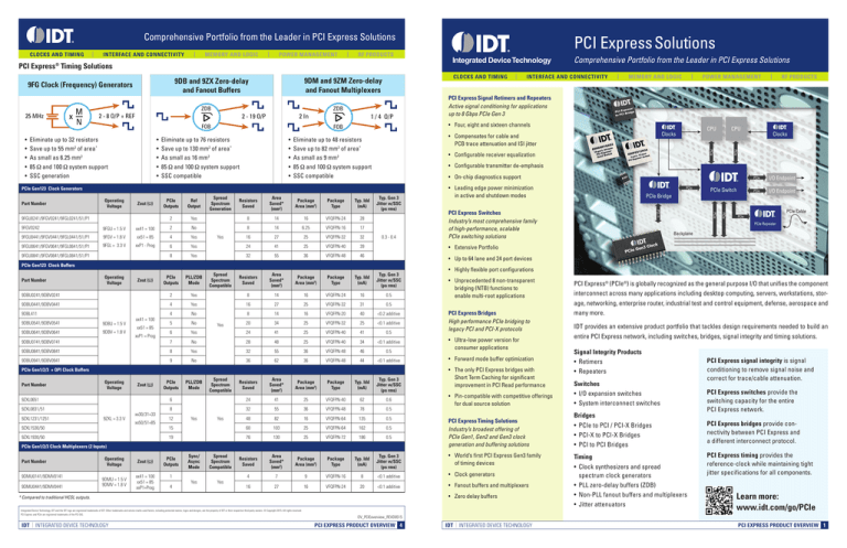
PCI Express® (PCIe®) is globally recognized as the general purpose I/O that unifies the component
interconnect across many applications including desktop computing, servers, workstations, storage, networking, enterprise router, industrial test and control equipment, defense, aerospace and
many more.
IDT provides an extensive product portfolio that tackles design requirements needed to build an
entire PCI Express network, including switches, bridges, signal integrity and timing solutions.
Signal Integrity Products
• Retimers
• Repeaters
• Pin-compatible with competitive offerings
for dual source solution
Switches
• I/O expansion switches
• System interconnect switches
PCI Express Timing Solutions
Industry’s broadest offering of
PCIe Gen1, Gen2 and Gen3 clock
generation and buffering solutions
Bridges
• PCIe to PCI / PCI-X Bridges
• PCI-X to PCI-X Bridges
• PCI to PCI Bridges
• Zero delay buffers
* Compared to traditional HCSL outputs.
IDT | INTEGRATED DEVICE TECHNOLOGY
PCI Express Bridges
High performance PCIe bridging to
legacy PCI and PCI-X protocols
Package
Area (mm2)
Spread
Spectrum
Compatible
PCIe Gen1/2/3 Clock Multiplexers (2 Inputs)
Part Number
• Unprecedented 8 non-transparent
bridging (NTB) functions to
enable multi-root applications
Area
Saved*
(mm2)
PLL/ZDB
Mode
6
9ZXL0831/51
• Highly flexible port configurations
Resistors
Saved
PCIe
Outputs
RF PRODUCTS
PCI Express Switches
Industry’s most comprehensive family
of high-performance, scalable
PCIe switching solutions
xx51 = 85
9DBL411
|
• Leading edge power minimization
in active and shutdown modes
xxP1 - Prog
Spread
Spectrum
Compatible
POWER MANAGEMENT
• On-chip diagnostics support
9FGV = 1.8 V
Zout ( )
|
• Configurable transmitter de-emphasis
9FGL = 3.3 V
Operating
Voltage
MEMORY AND LOGIC
• Configurable receiver equalization
9FGU0441/9FGV0441/9FGL0441/51/P1
Part Number
|
PCI Express Signal Retimers and Repeaters
Active signal conditioning for applications
up to 8 Gbps PCIe Gen 3
9FGU0641/9FGV0641/9FGL0641/51/P1
9FGU0841/9FGV0841/9FGL0841/51/P1
Yes
INTERFACE AND CONNECTIVITY
• Compensates for cable and
PCB trace attenuation and ISI jitter
Eliminate up to 48 resistors
Save up to 82 mm2 of area*
As small as 9 mm2
85 and 100 system support
SSC compatible
PCIe Gen123 Clock Generators
Part Number
|
• Four, eight and sixteen channels
FOB
Eliminate up to 76 resistors
Save up to 130 mm2 of area*
As small as 16 mm2
85 and 100 system support
SSC compatible
Integrated
DeviceTechnology
Integrated
DeviceTechnology Comprehensive Portfolio from the Leader in PCI Express Solutions
CLOCKS AND TIMING
9DM and 9ZM Zero-delay
and Fanout Multiplexers
9DB and 9ZX Zero-delay
and Fanout Buffers
9FG Clock (Frequency) Generators
PCI Express Solutions
Timing
• Clock synthesizers and spread
spectrum clock generators
• PLL zero-delay buffers (ZDB)
• Non-PLL fanout buffers and multiplexers
• Jitter attenuators
PCI Express signal integrity is signal
conditioning to remove signal noise and
correct for trace/cable attenuation.
PCI Express switches provide the
switching capacity for the entire
PCI Express network.
PCI Express bridges provide connectivity between PCI Express and
a different interconnect protocol.
PCI Express timing provides the
reference-clock while maintaining tight
jitter specifications for all components.
Learn more:
www.idt.com/go/PCIe
OV_PCIEoverview_REVD0515
PCI EXPRESS PRODUCT OVERVIEW 4
IDT | INTEGRATED DEVICE TECHNOLOGY
PCI EXPRESS PRODUCT OVERVIEW 1
Comprehensive Portfolio from the Leader in PCI Express Solutions
Integrated Device Technology
PCI Express Signal Integrity Products
PCIe Gen 3 and Gen2 Standards
With the increase of signal speeds in the
computing, storage and communications
applications, system designers increasingly
face signal integrity challenges. Signal Integrity Product (SIP) components provide
signal conditioning for applications up to
8 Gbps, PCI Express® 3.0, delivering signal
quality over extended distances while offering simplified design by alleviating board
layout constraints.
These devices incorporate advanced receive
equalization and transmit de-emphasis capabilities, as well as diagnostic features that
help IDT customers achieve a simplified design with faster time-to-market. Specifically,
the devices drive long on-board traces, backplane traces and cables to external devices
to ensure optimum system performance. The
devices all offer power savings modes for the
lowest-possible power consumption.
FEATURES
• Extends trace over 60 inches, and cable over 10 meters
• Eliminates Deterministic Jitter (Dj), Random Jitter (Rj) and Inter-Symbol Interference (ISI)
• Optimizes system performance by reducing lost packets
• Better system reliability with increased signal voltage and timing margins
• Simplifies system design and time-to-market
Part
Number
Channels
Pin Config
I2C Config
Package (mm)
Contact Pitch
(mm)
PCI Express® Switches
Part Number
PCIe
Specification
Lanes
Ports
Switch
Partitions
(Multi-root)
NTB Ports
DMA
Controllers
Multicast
Multi-Domain
Clocking
Package Size
(mm)
89H32NT24AG2
2
32
24
8
8
2
8
23 x 23
89H32NT8AG2
2
32
8
8
8
2
8
23 x 23
89H24NT6AG2
2
24
6
6
6
2
89H24NT24G2
2
24
24
8
8
2
6
23 x 23
2
23 x 23
89H16NT16G2
2
16
16
4
4
2
2
19 x 19
3
2
2
Yes
PCIe 3.0 Retimers
89H12NT12G2
2
12
12
3
89HT0808P
8
N
Y
9 x 9 BGA
0.8
89HPES64H16G2
2
64
16
16
89HT0816P
16
N
Y
15 x 15 BGA
1.0
89HPES48H12G2
2
48
12
12
89HPES32T8G2
2
32
8
23 x 23
89HPES24T6G2
2
24
6
19 x 19
89HT0816AP
16
N
Y
15 x 15 BGA
1.0
89HT0832P
32
N
Y
13 x 20 BGA
0.8
89HT0832P
32
N
Y
16 x 24 BGA
1.0
PCIe 2.1 Repeaters
19 x 19
35 x 35
27 x 27
89HPES24T3G2
2
24
3
19 x 19
89HPES16T4G2
2
16
4
23 x 23
89HPES12T3G2
2
12
3
89HPES6T6G2
2
6
6
N/A
N/A
N/A
N/A
19 x 19
N/A
89HP0504P
4
N
Y
4 x 7.5 QFN
0.5
89HP0504P
4
Y
Y
9 x 9 BGA
1.0
89HPES8T5A
1
8
5
15 x 15
89HP0504PB
4
Y
N
4 x 7.5 QFN
0.5
89HPES5T5
1
5
5
15 x 15
89HP0508P
8
N
Y
9 x 9 BGA
1.0
89HPES4T4
1
4
4
15 x 15
89HPES3T3
1
3
3
10 x 10
Additional products and information available — www.idt.com/go/PCIeSIP
19 x 19
Additional products and information available — www.idt.com/go/PCIeSwitches
PCI Express Switches
Featuring Dual DMA, Multiple NTB, Multicast; Configurations 3 to 64 Lanes and 3 to 24 Ports
IDT “I/O Expansion PCIe Switches” are commonly used to connect a single Root Complex
to I/O devices and add-in cards. In this usage
The other primary usage model is using a PCIe
switch as an embedded system fabric referred
to as “System Interconnect Switch,” which utilizes a high degree of peer-to-peer traffic. The
System Interconnect Switch is capable of PCIe
domain isolation, which may involve connecting multiple processing endpoints or simply
providing a redundant backplane architecture.
®
Example:
I/O Expansion
Server Motherboard
Chipset
Clock
Clock
CPU
®
®
Clock
Clock
Switch
Bridge
Clock
Switch
IDT | INTEGRATED DEVICE TECHNOLOGY
Example: System
Interconnect
Embedded Blade
CPU
PCI Express Bridges
µP Mezzanine
PCI-X 133 MHz
PCIe to PCI and PCI-X Bus Standards
To complement the switch products, IDT
offers bridges to connect PCIe to the PCI and
PCI-X bus standards. A PCIe bridge is used for
bridging devices that use the PCI/X interface
to provide a PCIe connection to a host processor or root complex. Applications include PCIe
adapter cards, embedded computing, and
motherboards to provide connection to PCI/X
devices or additional PCI/X expansion slots.
PCIe Slot
PCIe Slot
GbE/FC
Controller
PCI
PEB383
10x10 mm
footprint supports
up to four PCI
devices off x1 PCIe
®
PCIe
Tsi384
PCIe x4
PCI-X 133 MHz
Graphics
GbE/FC
Controller
Memory
PCIe Slot
Processor
Chipset
Peripherals
CPU
Example: Motherboard Application
Example: Storage HBA
Bridge
Part Number
PCIe I/F
PCI Speed
(MHz)
External
Master Support
Power
Package
(mm)
PCIe to PCI
89HPEB383
x1 Gen1
32/66
4
450 mW
14 x 14 QFP
10 x 10 QFN
PCIe to PCI
Tsi381
x1 Gen1
32/66
4
700 mW
13 x 13 PBGA
PCIe to PCI
Tsi382
x1 Gen1
32/66
4
700 mW
20 x 20 QFP
10 x 10 PBGA
PCIe to PCI-X
Tsi384
x4 Gen1
64/133
4
1.3 W
17 x 17 PBGA
PCI to PCI
Tsi340
32/66
4
500 mW
23 x 17 QFP
• Small footprint packages
PCI to PCI
Tsi350
32/66
9
1.0 W
31 x 31 QFP
17 x 17 BGA
• Simple power supply requirements
PCI to PCI
Tsi352
32/66
4
500 mW
32 x 32 QFP
FEATURES
• Compliant to PCIe 1.1 specification
• Low latency & high throughput
features
• Proven interoperability
NTB
To Backplane
2
Memory
Memory
Memory
CPU
Clock
model, the majority of traffic flows between
the Root Complex and the I/O devices.
NTB
IDT provides the industry’s most comprehensive family of high performance, scalable PCI
Express switching solutions. PCIe® switching solutions are optimized by application to
maximize performance per watt for the most
demanding applications.
FEATURES
• Most advanced switching
architecture available
– Switch partitioning
– Adaptive cut-through latency
– Request metering
– Large flow control credits and buffers
• Enables multi-domain communication
in multi-root applications
– Multiple non-transparent
bridge functions
– Multi-port timing domain and
spread spectrum clock support
– Multicast
– Dual DMA controllers
• Comprehensive design tools
N/A
Contact an IDT representative for details on pin-compatibility with comparable solutions.
Additional products and information available — www.idt.com/go/PCIeBridges
PCI EXPRESS PRODUCT OVERVIEW 3
Comprehensive Portfolio from the Leader in PCI Express Solutions
Integrated DeviceTechnology
CLOCKS AND TIMING
|
INTERFACE AND CONNECTIVITY
|
MEMORY AND LOGIC
|
POWER MANAGEMENT
|
RF PRODUCTS
PCI Express® Timing Solutions
25 MHz
•
•
•
•
•
x
M
N
ZDB
ZDB
2 - 8 O/P + REF
2 In
2 - 19 O/P
1 / 4 O/P
FOB
Eliminate up to 32 resistors
Save up to 55 mm2 of area*
As small as 6.25 mm2
85 and 100 system support
SSC generation
•
•
•
•
•
•
•
•
•
•
Operating
Voltage
Zout ( )
9FGU0241/9FGV0241/9FGL0241/51/P1
9FGV0242
9FGU = 1.5 V
xx41 = 100
Spread
Spectrum
Generation
Resistors
Saved
Area
Saved*
(mm2)
Package
Area (mm2)
Package
Type
Typ. Idd
(mA)
Yes
8
14
16
VFQFPN-24
28
No
8
14
6.25
VFQFPN-16
17
PCIe
Outputs
Ref
Output
2
2
Typ. Gen 3
Jitter w/SSC
(ps rms)
4
Yes
16
27
25
VFQFPN-32
32
6
Yes
24
41
25
VFQFPN-40
39
• Extensive Portfolio
8
Yes
32
55
36
VFQFPN-48
46
0.3 - 0.4
• Up to 64 lane and 24 port devices
PCIe
Outputs
PLL/ZDB
Mode
Resistors
Saved
Area
Saved*
(mm2)
Package
Area (mm2)
Package
Type
Typ. Idd
(mA)
PCIe Gen123 Clock Buffers
Typ. Gen 3
Jitter w/SSC
(ps rms)
9DBU0241/9DBV0241
2
Yes
8
14
16
VFQFPN-24
16
0.5
9DBU0441/9DBV0441
4
Yes
16
27
25
VFQFPN-32
31
0.5
4
No
8
14
16
VFQFPN-20
40
<0.2 additive
9DBU0541/9DBV0541
9DBU = 1.5 V
9DBU0641/9DBV0641
9DBV = 1.8 V
xx41 = 100
5
No
20
34
25
VFQFPN-32
25
<0.1 additive
6
Yes
24
41
25
VFQFPN-40
41
0.5
7
No
28
48
25
VFQFPN-40
34
<0.1 additive
9DBU0841/9DBV0841
8
Yes
32
55
36
VFQFPN-48
46
0.5
9DBU0941/9DBV0941
9
No
36
62
36
VFQFPN-48
44
<0.1 additive
9DBU0741/9DBV0741
xx51 = 85
xxP1 = Prog
Yes
PCIe Gen1/2/3 + QPI Clock Buffers
Part Number
Operating
Voltage
Zout ( )
9ZXL0651
9ZXL1231/1251
9ZXL = 3.3 V
9ZXL1530/50
xx30/31=33
xx50/51=85
9ZXL1930/50
9DMU0141/9DMV0141
9DMU0441/9DMV0441
Operating
Voltage
Zout ( )
9DMU = 1.5 V
9DMV = 1.8 V
xx41 = 100
xx51 = 85
xxP1=Prog
• Ultra-low power version for
consumer applications
• Forward mode buffer optimization
• The only PCI Express bridges with
Short Term Caching for significant
improvement in PCI Read performance
Package
Type
Typ. Idd
(mA)
Typ. Gen 3
Jitter w/SSC
(ps rms)
24
41
25
VFQFPN-40
62
0.6
32
55
36
VFQFPN-48
78
0.5
48
82
16
VFQFPN-64
135
0.5
15
60
103
25
VFQFPN-64
162
0.5
19
76
130
25
VFQFPN-72
186
0.5
Resistors
Saved
Area
Saved*
(mm2)
Package
Area (mm2)
Package
Type
Typ. Idd
(mA)
Typ. Gen 3
Jitter w/SSC
(ps rms)
• World’s first PCI Express Gen3 family
of timing devices
4
7
9
VFQFPN-16
8
<0.1 additive
• Clock generators
16
27
16
VFQFPN-24
20
<0.1 additive
• Fanout buffers and multiplexers
8
12
Yes
Yes
PCIe
Outputs
1
4
Sync/
Async
Mode
Spread
Spectrum
Compatible
Yes
Yes
Integrated Device Technology, IDT and the IDT logo are registered trademarks of IDT. Other trademarks and service marks used herein, including protected names, logos and designs, are the property of IDT or their respective third party owners. © Copyright 2015. All rights reserved.
PCI Express and PCIe are registered trademarks of the PCI-SIG.
PCI Express® (PCIe®) is globally recognized as the general purpose I/O that unifies the component
interconnect across many applications including desktop computing, servers, workstations, storage, networking, enterprise router, industrial test and control equipment, defense, aerospace and
many more.
IDT provides an extensive product portfolio that tackles design requirements needed to build an
entire PCI Express network, including switches, bridges, signal integrity and timing solutions.
Signal Integrity Products
• Retimers
• Repeaters
• Pin-compatible with competitive offerings
for dual source solution
Switches
• I/O expansion switches
• System interconnect switches
PCI Express Timing Solutions
Industry’s broadest offering of
PCIe Gen1, Gen2 and Gen3 clock
generation and buffering solutions
Bridges
• PCIe to PCI / PCI-X Bridges
• PCI-X to PCI-X Bridges
• PCI to PCI Bridges
• Zero delay buffers
* Compared to traditional HCSL outputs.
IDT | INTEGRATED DEVICE TECHNOLOGY
PCI Express Bridges
High performance PCIe bridging to
legacy PCI and PCI-X protocols
Package
Area (mm2)
Spread
Spectrum
Compatible
PCIe Gen1/2/3 Clock Multiplexers (2 Inputs)
Part Number
• Unprecedented 8 non-transparent
bridging (NTB) functions to
enable multi-root applications
Area
Saved*
(mm2)
PLL/ZDB
Mode
6
9ZXL0831/51
• Highly flexible port configurations
Resistors
Saved
PCIe
Outputs
RF PRODUCTS
PCI Express Switches
Industry’s most comprehensive family
of high-performance, scalable
PCIe switching solutions
xx51 = 85
9DBL411
|
• Leading edge power minimization
in active and shutdown modes
xxP1 - Prog
Spread
Spectrum
Compatible
POWER MANAGEMENT
• On-chip diagnostics support
9FGV = 1.8 V
Zout ( )
|
• Configurable transmitter de-emphasis
9FGL = 3.3 V
Operating
Voltage
MEMORY AND LOGIC
• Configurable receiver equalization
9FGU0441/9FGV0441/9FGL0441/51/P1
Part Number
|
PCI Express Signal Retimers and Repeaters
Active signal conditioning for applications
up to 8 Gbps PCIe Gen 3
9FGU0641/9FGV0641/9FGL0641/51/P1
9FGU0841/9FGV0841/9FGL0841/51/P1
Yes
INTERFACE AND CONNECTIVITY
• Compensates for cable and
PCB trace attenuation and ISI jitter
Eliminate up to 48 resistors
Save up to 82 mm2 of area*
As small as 9 mm2
85 and 100 system support
SSC compatible
PCIe Gen123 Clock Generators
Part Number
|
• Four, eight and sixteen channels
FOB
Eliminate up to 76 resistors
Save up to 130 mm2 of area*
As small as 16 mm2
85 and 100 system support
SSC compatible
Integrated
DeviceTechnology
Integrated
DeviceTechnology Comprehensive Portfolio from the Leader in PCI Express Solutions
CLOCKS AND TIMING
9DM and 9ZM Zero-delay
and Fanout Multiplexers
9DB and 9ZX Zero-delay
and Fanout Buffers
9FG Clock (Frequency) Generators
PCI Express Solutions
Timing
• Clock synthesizers and spread
spectrum clock generators
• PLL zero-delay buffers (ZDB)
• Non-PLL fanout buffers and multiplexers
• Jitter attenuators
PCI Express signal integrity is signal
conditioning to remove signal noise and
correct for trace/cable attenuation.
PCI Express switches provide the
switching capacity for the entire
PCI Express network.
PCI Express bridges provide connectivity between PCI Express and
a different interconnect protocol.
PCI Express timing provides the
reference-clock while maintaining tight
jitter specifications for all components.
Learn more:
www.idt.com/go/PCIe
OV_PCIEoverview_REVD0515
PCI EXPRESS PRODUCT OVERVIEW 4
IDT | INTEGRATED DEVICE TECHNOLOGY
PCI EXPRESS PRODUCT OVERVIEW 1
