EV0020 (MP1591DN)
2A, 32V, 330KHz
Step-Down Converter
The Future of Analog IC Technology
EVALUATION BOARD
DESCRIPTION
FEATURES
The EV0020 is the evaluation board for the
MP1591; a high voltage step-down converter
ideal for automotive power adapter battery
chargers. Its wide 6.5V to 32V input voltage
range covers the automotive battery’s
requirements. It achieves 2A continuous output
for quick charge capability.
•
•
•
•
•
•
•
•
•
•
•
Current mode operation provides fast transient
response and eases loop stabilization. Fault
protection includes cycle-by-cycle current
limiting and thermal shutdown. In shutdown
mode, the converter draws only 20µA of supply
current.
Wide 6.5V to 32V Input Operating Range
34V Absolute Maximum Input
2A Output Current
Ceramic Input and Output Capacitors
Up to 95% Efficiency
20µA Shutdown Mode
Fixed 330KHz Frequency
Thermal Shutdown
Cycle-by-Cycle Over Current Protection
Output Adjustable From 1.23V to 21V
Under Voltage Lockout
APPLICATIONS
The MP1591 requires a minimum number of
readily available external components to
complete a 2A step-down DC to DC converter
solution.
•
•
•
•
ELECTRICAL SPECIFICATIONS
“MPS” and “The Future of Analog IC Technology” are Registered Trademarks of
Monolithic Power Systems, Inc.
Parameter
Input Voltage
Output Voltage
Output Current
Symbol
Value
Units
VIN
VOUT
IOUT
6.5 to 32
5
2
V
V
A
Automotive Power Adapters
PDA and Cellular Phone Battery Chargers
Distributed Power Systems
Automotive Aftermarket Electronics
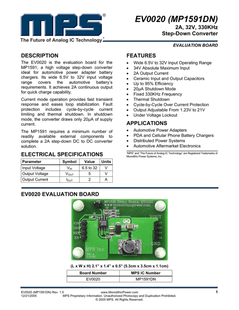
EV0020 EVALUATION BOARD
(L x W x H) 2.1” x 1.4” x 0.5” (5.3cm x 3.5cm x 1.1cm)
Board Number
MPS IC Number
EV0020
MP1591DN
EV0020 (MP1591DN) Rev. 1.5
www.MonolithicPower.com
12/21/2005
MPS Proprietary Information. Unauthorized Photocopy and Duplication Prohibited.
© 2005 MPS. All Rights Reserved.
1
EV0020 (MP1591DN) – 2A, 32V, 330KHz STEP-DOWN CONVERTER
EVALUATION BOARD
EVALUATION BOARD SCHEMATIC
VIN
JP1
OFF
GND
U1
VIN
EN
EN
BS
MP1591
REF
C6
NS
REF
SW
COMP
FB
C3
1.8nF
C1
10nF
VOUT
D1
B340A-13
GND
GND
C4
NS
EV0020_S01
EV0020 BILL OF MATERIALS
Qty
Ref
Value
Description
1
1
1
2
1
C1
C2
C3
C4, C6
C5
10nF
10µF
1.8nF
NS
22µF
1
D1
1
1
1
1
R1
R2
R3
L1
L1
Alternate
U1
47kΩ
8.2kΩ
15kΩ
22µH
Ceramic Capacitor, 50V, X7R
Ceramic Capacitor, 35V
Ceramic Capacitor, 50V, X7R
Not Stuffed
Ceramic Capacitor, 10V, 1210
Schottky Diode,
40V, 3A, SMA
Film Resistor, 1%
Film Resistor, 5%
Film Resistor, 1%
Inductor, 2.6A
22µH
Inductor, 2.5A, Type D104C
1
Step-Down Converter
Package Manufacturer
Manufacturer P/N
0805
1210
0805
AVX
Taiyo Yuden
AVX
08055C103KAT2A
GMK325F106MH
08055C182KAT2A
1210
Taiyo Yuden
LMK325BJ226MM
Diodes Inc
B340A-13
Yageo
Panasonic
Yageo
Sumida
9C08052A4702FKHFT
ERJ-6GEYJ822V
9C08052A1502FKHFT
CDRH8D43-220
Toko
919AS-220M
MPS
MP1591DN
0805
0805
0805
SO8
EV0020 (MP1591DN) Rev. 1.5
www.MonolithicPower.com
12/21/2005
MPS Proprietary Information. Unauthorized Photocopy and Duplication Prohibited.
© 2005 MPS. All Rights Reserved.
2
EV0020 (MP1591DN) – 2A, 32V, 330KHz STEP-DOWN CONVERTER
EVALUATION BOARD
PRINTED CIRCUIT BOARD LAYOUT
Figure 1—Top Silk Layer
Figure 2—Top Layer
Figure 3—Bottom Layer
EV0020 (MP1591DN) Rev. 1.5
www.MonolithicPower.com
12/21/2005
MPS Proprietary Information. Unauthorized Photocopy and Duplication Prohibited.
© 2005 MPS. All Rights Reserved.
3
EV0020 (MP1591DN) – 2A, 32V, 330KHz STEP-DOWN CONVERTER
EVALUATION BOARD
QUICK START GUIDE
The output voltage of this board is set to 5V. The board layout accommodates most commonly used
inductors and output capacitors.
1. Attach the positive and negative ends of the load to VOUT and GND, respectively.
2. Attach the input voltage (6.5V ≤ VIN ≤ 32V) and input ground to VIN and GND, respectively.
3. To enable to the MP1591, apply a voltage (VEN ≥ 2V) to the EN pin. To disable it, connect the
EN pin to ground.
4. The REF pin outputs a 5V reference voltage. If used, a 0.01µF capacitor should be connected
from this pin to GND to reduce switching ripple. Leave unconnected if not used.
5. The output voltage VOUT can be changed by varying R1. Calculate R1 using the formula:
⎛V
⎞
R1 = R3 × ⎜⎜ OUT − 1⎟⎟ where VFB = 1.23V and R3 is set at 15kΩ.
V
⎝ FB
⎠
For example, for VOUT = 5.0V:
⎛V
⎞
⎛ 5 .0 V
⎞
R1 = R3 × ⎜⎜ OUT − 1⎟⎟ = 15kΩ × ⎜
− 1⎟ = 45.98kΩ ≈ 47kΩ standard 1% value.
⎝ 1.23 V
⎠
⎝ VFB
⎠
See Maximum Duty Cycle limits to determine allowable output voltage range.
NOTICE: The information in this document is subject to change without notice. Please contact MPS for current specifications.
Users should warrant and guarantee that third party Intellectual Property rights are not infringed upon when integrating MPS
products into any application. MPS will not assume any legal responsibility for any said applications.
EV0020 (MP1591DN) Rev. 1.5
www.MonolithicPower.com
12/21/2005
MPS Proprietary Information. Unauthorized Photocopy and Duplication Prohibited.
© 2005 MPS. All Rights Reserved.
4
