MP9942
The Future of Analog IC Technology
High Efficiency 2A, 36V, 410kHz
Synchronous Step-Down Converter
with Power Good
DESCRIPTION
FEATURES
The MP9942 is a high-frequency, synchronous,
rectified, step-down, switch-mode converter
with built-in power MOSFETs. It offers a very
compact solution to achieve a 2A continuous
output current with excellent load and line
regulation over a wide input supply range. The
MP9942 has synchronous mode operation for
higher efficiency over the output current load
range.
•
Current-mode operation provides fast transient
response and eases loop stabilization.
Full protection features include over-current
protection and thermal shutdown.
The MP9942 requires a minimal number of
readily-available standard external components,
and is available in a space-saving 8-pin
TSOT23 package.
•
•
•
•
•
•
•
•
•
•
•
•
•
Wide 4V to 30V Continuous Operating Input
Range
36V Input Transient Tolerance
90mΩ/55mΩ Low RDS(ON) Internal Power
MOSFETs
High-Efficiency Synchronous Mode
Operation
410kHz Switching Frequency
Synchronizes from 200kHz to 2.2MHz
External Clock
High Duty Cycle for Automotive Cold-crank
Internal Power-Save Mode
Internal Soft-Start
Power Good Indicator
Over-Current Protection with Hiccup
Thermal Shutdown
Output Adjustable from 0.8V
Available in an 8-pin TSOT-23 package
APPLICATIONS
•
•
•
Automotive
Industrial Control System
Distributed Power Systems
All MPS parts are lead-free and adhere to the RoHS directive. For MPS green
status, please visit MPS website under Quality Assurance. “MPS” and “The
Future of Analog IC Technology” are Registered Trademarks of Monolithic
Power Systems, Inc.
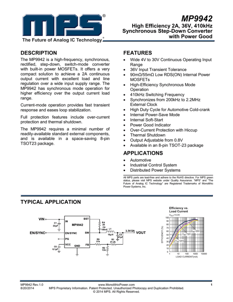
TYPICAL APPLICATION
MP9942 Rev.1.0
8/20/2014
www.MonolithicPower.com
MPS Proprietary Information. Patent Protected. Unauthorized Photocopy and Duplication Prohibited.
© 2014 MPS. All Rights Reserved.
1
MP9942 – 36V, 2A SYNCHRONOUS STEP-DOWN CONVERTER
ORDERING INFORMATION
Part Number*
MP9942GJ
Package
TSOT23-8
Top Marking
See Below
* For Tape & Reel, add suffix –Z (e.g. MP9942GJ–Z);
TOP MARKING
ALL: product code of MP9942GJ;
Y: year code;
PACKAGE REFERENCE
TOP VIEW
PG
1
8
FB
IN
2
7
VCC
SW
3
6
EN/SYNC
GND
4
5
BST
TSOT23-8
MP9942 Rev.1.0
8/8/2014
www.MonolithicPower.com
MPS Proprietary Information. Patent Protected. Unauthorized Photocopy and Duplication Prohibited.
© 2014 MPS. All Rights Reserved.
2
MP9942 – 36V, 2A SYNCHRONOUS STEP-DOWN CONVERTER
ABSOLUTE MAXIMUM RATINGS (1)
Thermal Resistance
VIN ..................................................-0.3V to 40V
VSW ..................................................-0.3V to 41V
VBS ......................................................... VSW+6V
All Other Pins ................................ -0.3V to 6V (2)
(3)
Continuous Power Dissipation (TA = +25°C)
TSOT23-8 ................................................ 1.25W
Junction Temperature ...............................150°C
Lead Temperature ....................................260°C
Storage Temperature................. -65°C to 150°C
TSOT23-8.............................. 100 ..... 55... °C/W
Recommended Operating Conditions
(4)
Continuous Supply Voltage VIN ...........4V to 30V
Output Voltage VOUT ..................0.8V to VIN*DMAX
Operating Junction Temp. (TJ). -40°C to +125°C
MP9942 Rev.1.0
8/8/2014
(5)
θJA
θJC
Notes:
1) Absolute maximum ratings are rated under room temperature
unless otherwise noted. Exceeding these ratings may
damage the device.
2) About the details of EN pin’s ABS MAX rating, please refer to
page 14, Enable/SYNC control section.
3) The maximum allowable power dissipation is a function of the
maximum junction temperature TJ (MAX), the junction-toambient thermal resistance θJA, and the ambient temperature
TA. The maximum allowable continuous power dissipation at
any ambient temperature is calculated by PD (MAX) = (TJ
(MAX)-TA)/θJA. Exceeding the maximum allowable power
dissipation will cause excessive die temperature, and the
regulator will go into thermal shutdown. Internal thermal
shutdown circuitry protects the device from permanent
damage.
4) The device is not guaranteed to function outside of its
operating conditions.
5) Measured on JESD51-7, 4-layer PCB.
www.MonolithicPower.com
MPS Proprietary Information. Patent Protected. Unauthorized Photocopy and Duplication Prohibited.
© 2014 MPS. All Rights Reserved.
3
MP9942 – 36V, 2A SYNCHRONOUS STEP-DOWN CONVERTER
ELECTRICAL CHARACTERISTICS
VIN = 12V, TJ = +25°C, unless otherwise noted.
Parameter
Symbol
Supply Current (Shutdown)
ISHDN
Supply Current (Quiescent)
IQ
HS Switch-ON Resistance
Condition
Min
Typ
VEN = 0V
Max
Units
8
μA
VEN = 2V, VFB = 1V
0.5
0.7
mA
RON_HS
VBST-SW=5V
90
155
mΩ
LS Switch-ON Resistance
RON_LS
VCC =5V
55
105
mΩ
Switch Leakage
ILKG_SW
VEN = 0V, VSW =12V
1
μA
Current Limit
ILIMIT
Oscillator Frequency
fSW
Fold-Back Frequency
Maximum Duty Cycle
fFB
DMAX
Minimum ON Time(6)
tON_MIN
Under 40% Duty Cycle
3
4.2
5.5
A
VFB=750mV
320
410
500
kHz
VFB<400mV
VFB=750mV, 410kHz
70
92
100
95
130
kHz
%
2.4
MHz
792
804
mV
10
100
nA
70
Sync Frequency Range
fSYNC
0.2
Feedback Voltage
VFB
780
Feedback Current
IFB
VFB=820mV
ns
EN Rising Threshold
VEN_RISING
1.15
1.4
1.65
V
EN Falling Threshold
VEN_FALLING
1.05
1.25
1.45
V
EN Threshold Hysteresis
EN Input Current
VEN_HYS
IEN
VIN Under-Voltage Lockout
Threshold-Rising
VIN Under-Voltage Lockout
Threshold-Falling
VIN Under-Voltage Lockout
Threshold-Hysteresis
VCC Regulator
VEN=2V
4
6
μA
VEN=0
0
0.2
μA
3.3
3.5
3.7
V
INUVFALLING
3.1
3.3
3.5
V
INUVHYS
VCC Load Regulation
200
ICC=0mA
4.6
tSS
Thermal Shutdown (6)
TSD
VOUT from 10% to 90%
mV
4.9
5.2
V
1.5
4
%
0.55
1.45
2.45
ms
150
170
°C
30
°C
ICC=5mA
Soft-Start Period
Thermal Hysteresis
mV
INUVRISING
VCC
(6)
150
TSD_HYS
PG Rising Threshold
PGVth_RISING
as percentage of VFB
86.5
90
93.5
%
PG Falling Threshold
PGVth_FALLING
as percentage of VFB
80.5
84
87.5
%
MP9942 Rev.1.0
8/8/2014
www.MonolithicPower.com
MPS Proprietary Information. Patent Protected. Unauthorized Photocopy and Duplication Prohibited.
© 2014 MPS. All Rights Reserved.
4
MP9942 – 36V, 2A SYNCHRONOUS STEP-DOWN CONVERTER
ELECTRICAL CHARACTERISTICS (continued)
VIN = 12V, TJ = +25°C, unless otherwise noted.
Parameter
Symbol
Condition
PG Threshold Hysteresis
PGVth_HYS
as percentage of VFB
Min
Typ
Max
6
Units
%
PG Rising Delay
PGTd_RISING
40
90
160
μs
PG Falling Delay
PGTd_FALLING
30
55
95
μs
0.1
0.3
V
10
100
nA
PG Sink Current Capability
PG Leakage Current
VPG
Sink 4mA
ILKG_PG
Notes:
6) Derived from bench characterization. Not tested in production
MP9942 Rev.1.0
8/8/2014
www.MonolithicPower.com
MPS Proprietary Information. Patent Protected. Unauthorized Photocopy and Duplication Prohibited.
© 2014 MPS. All Rights Reserved.
5
MP9942 – 36V, 2A SYNCHRONOUS STEP-DOWN CONVERTER
PIN FUNCTIONS
Package
Pin #
1
2
3
4
5
6
7
8
Name
Description
Power Good. The output of this pin is an open drain and goes high if the output voltage
exceeds 90% of the nominal voltage.
Supply Voltage. The MP9942 operates from a 4V to 30V input rail. Requires C1 to
IN
decouple the input rail. Connect using a wide PCB trace.
SW
Switch Output. Connect with a wide PCB trace.
System Ground. This pin is the reference ground of the regulated output voltage, and PCB
GND
layout requires special care. For best results, connect to GND with copper traces and vias.
Bootstrap. Requires a capacitor connected between SW and BST pins to form a floating
BST
supply across the high-side switch driver. A 20Ω resistor placed between SW and BST cap
is strongly recommended to reduce SW spike voltage.
Enable/Synchronize. EN/SYNC high to enable the MP9942. Apply an external clock to the
EN/SYNC
EN/SYNC pin to change the switching frequency.
Bias Supply. Decouple with 0.1μF-to-0.22μF capacitor. Select a capacitor that does not
VCC
exceed 0.22μF
Feedback. Connect to the tap of an external resistor divider from the output to GND, to set
the output voltage. The frequency fold-back comparator lowers the oscillator frequency
FB
when the FB voltage is below 660mV to prevent current limit runaway during a short-circuit
fault condition.
MP9942 Rev.1.0
8/8/2014
PG
www.MonolithicPower.com
MPS Proprietary Information. Patent Protected. Unauthorized Photocopy and Duplication Prohibited.
© 2014 MPS. All Rights Reserved.
6
MP9942 – 36V, 2A SYNCHRONOUS STEP-DOWN CONVERTER
TYPICAL CHARACTERISTICS
MP9942 Rev.1.0
8/8/2014
www.MonolithicPower.com
MPS Proprietary Information. Patent Protected. Unauthorized Photocopy and Duplication Prohibited.
© 2014 MPS. All Rights Reserved.
7
MP9942 – 36V, 2A SYNCHRONOUS STEP-DOWN CONVERTER
TYPICAL CHARACTERISTICS (continued)
MP9942 Rev.1.0
8/8/2014
www.MonolithicPower.com
MPS Proprietary Information. Patent Protected. Unauthorized Photocopy and Duplication Prohibited.
© 2014 MPS. All Rights Reserved.
8
MP9942 – 36V, 2A SYNCHRONOUS STEP-DOWN CONVERTER
TYPICAL PERFORMANCE CHARACTERISTICS
VIN = 12V, VOUT = 3.3V, L = 10µH, RBST=20Ω, TA = +25°C, unless otherwise noted.
MP9942 Rev.1.0
8/8/2014
www.MonolithicPower.com
MPS Proprietary Information. Patent Protected. Unauthorized Photocopy and Duplication Prohibited.
© 2014 MPS. All Rights Reserved.
9
MP9942 – 36V, 2A SYNCHRONOUS STEP-DOWN CONVERTER
TYPICAL PERFORMANCE CHARACTERISTICS (continued)
VIN = 12V, VOUT = 3.3V, L = 10µH, RBST=20Ω, TA = +25°C, unless otherwise noted.
MP9942 Rev.1.0
8/8/2014
www.MonolithicPower.com
MPS Proprietary Information. Patent Protected. Unauthorized Photocopy and Duplication Prohibited.
© 2014 MPS. All Rights Reserved.
10
MP9942 – 36V, 2A SYNCHRONOUS STEP-DOWN CONVERTER
TYPICAL PERFORMANCE CHARACTERISTICS (continued)
VIN = 12V, VOUT = 3.3V, L = 10µH, RBST=20Ω, TA = +25°C, unless otherwise noted.
MP9942 Rev.1.0
8/8/2014
www.MonolithicPower.com
MPS Proprietary Information. Patent Protected. Unauthorized Photocopy and Duplication Prohibited.
© 2014 MPS. All Rights Reserved.
11
MP9942 – 36V, 2A SYNCHRONOUS STEP-DOWN CONVERTER
TYPICAL PERFORMANCE CHARACTERISTICS (continued)
VIN = 12V, VOUT = 3.3V, L = 10µH, RBST=20Ω, TA = +25°C, unless otherwise noted.
MP9942 Rev.1.0
8/8/2014
www.MonolithicPower.com
MPS Proprietary Information. Patent Protected. Unauthorized Photocopy and Duplication Prohibited.
© 2014 MPS. All Rights Reserved.
12
MP9942 – 36V, 2A SYNCHRONOUS STEP-DOWN CONVERTER
FUNCTIONAL BLOCK DIAGRAM
Figure 1: Functional Block Diagram
MP9942 Rev.1.0
8/8/2014
www.MonolithicPower.com
MPS Proprietary Information. Patent Protected. Unauthorized Photocopy and Duplication Prohibited.
© 2014 MPS. All Rights Reserved.
13
MP9942 – 36V, 2A SYNCHRONOUS STEP-DOWN CONVERTER
OPERATION
The MP9942 is a high-frequency, synchronous,
rectified, step-down, switch-mode converter with
built-in power MOSFETs. It offers a very compact
solution to achieve 2A continuous output current
with excellent load and line regulation over a
wide input supply range.
When MP9942 operates in a fixed-frequency,
peak-current–control mode to regulate the output
voltage, an internal clock initiates a PWM cycle.
The integrated high-side power MOSFET turns
on and remains on until its current reaches the
value set by the COMP voltage. When the power
switch is off, it remains off until the next clock
cycle starts. If the current in the power MOSFET
does not reach the current value set by COMP
within 95% of one PWM period, the power
MOSFET will be forced to turn off.
Internal Regulator
The 5V internal regulator power most of the
internal circuitries. This regulator is supplied by
the VIN input and operates in the full VIN range:
When VIN exceeds 5.0V, the output of the
regulator is in full regulation; when VIN falls below
5.0V, the output of the regulator decreases
following the VIN. A 0.1uF decoupling ceramic
capacitor is needed at the pin.
Error Amplifier
The error amplifier compares the FB pin voltage
against the internal 0.792V reference (REF) and
outputs a COMP voltage—this COMP voltage
controls the power MOSFET current. The
optimized
internal
compensation
network
minimizes the external component count and
simplifies the control loop design.
Power Save Mode for Light Load Condition
The MP9942 has AAM (Advanced Asynchronous
Modulation) power-save mode for light load. The
AAM threshold is fixed internally. Under the
heavy load condition, the VCOMP is higher than
VAAM. When the clock goes high, the high-side
power MOSFET turns on and remains on until
VILsense reaches the value set by the COMP
voltage. The internal clock resets every time
when VCOMP is higher than VAAM.
Under the light load condition, the value of VCOMP
is low. When VCOMP is less than VAAM and VFB is
MP9942 Rev.1.0
8/8/2014
less than VREF, VCOMP ramps up until it exceeds
VAAM. During this time, the internal clock is
blocked, thus the MP9942 skips some pulses for
PFM (Pulse Frequency Modulation) mode and
achieves the light load power save.
Figure 2: Simplified AAM Control Logic
Enable/SYNC control
EN/SYNC is a digital control pin that turns the
regulator on and off: Drive EN/SYNC high to turn
on the regulator, drive it low to turn it off. An
internal 500kΩ resistor from EN/SYNC to GND
allows EN/SYNC to be floated to shut down the
chip.
The EN/SYNC pin is clamped internally using a
6.5V series Zener diode, as shown in Figure 3.
Connect the EN/SYNC pin through a pullup
resistor to any voltage connected to the VIN pin—
the pullup resistor limits the EN/SYNC input
current to less than 100µA.
For example, with 12V connected to VIN, RPULLUP
≥ (12V – 6.5V) ÷ 100µA = 55kΩ.
Connecting the EN/SYNC pin directly to a voltage
source without any pullup resistor requires
limiting voltage amplitude to ≤6V to prevent
damage to the Zener diode.
Figure 3: 6.5V-type Zener Diode
Connect an external clock with a range of
200kHz to 2.2MHz to synchronize the internal
clock rising edge to the external clock rising edge.
The pulse width of external clock signal should
be less than 2μs.
www.MonolithicPower.com
MPS Proprietary Information. Patent Protected. Unauthorized Photocopy and Duplication Prohibited.
© 2014 MPS. All Rights Reserved.
14
MP9942 – 36V, 2A SYNCHRONOUS STEP-DOWN CONVERTER
Under-Voltage Lockout
Under-voltage lockout (UVLO) protects the chip
from operating at an insufficient supply voltage.
The MP9942 UVLO comparator monitors the
output voltage of the internal regulator, VCC. The
UVLO rising threshold is about 3.5V while its
falling threshold is 3.3V.
Internal Soft-Start
The soft-start prevents the converter output
voltage from overshooting during startup. When
the chip starts, the internal circuitry generates a
soft-start voltage (SS) that ramps up from 0V to
1.2V. When SS is lower than REF, SS overrides
REF so the error amplifier uses SS as the
reference. When SS exceeds REF, the error
amplifier uses REF as the reference. The SS
time is internally set to 1.45ms.
Over-Current Protection and Hiccup
The MP9942 has cycle-by-cycle over current limit
when the inductor current peak value exceeds
the set current limit threshold. If the output
voltage starts to drop until FB is below the UnderVoltage (UV) threshold—typically 84% below the
reference—the MP9942 enters hiccup mode to
periodically restart the part. This protection mode
is especially useful when the output is deadshorted to ground. The average short-circuit
current is greatly reduced to alleviate the thermal
issue and to protect the regulator. The MP9942
exits the hiccup mode once the over-current
condition is removed.
Thermal Shutdown
Thermal shutdown prevents the chip from
operating at exceedingly high temperatures.
When the silicon die temperature exceeds 170°C,
it shuts down the whole chip. When the
temperature drops below its lower threshold
(typically 140°C) the chip is enabled again.
Floating Driver and Bootstrap Charging
An external bootstrap capacitor powers the
floating power MOSFET driver. This floating
driver has its own UVLO protection, with a rising
threshold of 2.2V and hysteresis of 150mV. The
bootstrap capacitor voltage is regulated internally
by VIN through D1, M1, C4, L1 and C2 (Figure ).
If (VIN-VSW) exceeds 5V, U1 regulates M1 to
maintain a 5V BST voltage across C4. A 20Ω
resistor placed between SW and BST cap is
MP9942 Rev.1.0
8/8/2014
strongly recommended to reduce SW spike
voltage.
Figure 4: Internal Bootstrap Charging Circuit
Startup and Shutdown
If both VIN and EN exceed their appropriate
thresholds, the chip starts: The reference block
starts first, generating stable reference voltage
and currents, and then the internal regulator is
enabled. The regulator provides stable supply for
the remaining circuitries.
Three events can shut down the chip: EN low, VIN
low, and thermal shutdown. In the shutdown
procedure, the signaling path is first blocked to
avoid any fault triggering. The COMP voltage and
the internal supply rail are then pulled down. The
floating driver is not subject to this shutdown
command.
Power Good
The MP9942 has power good (PG) output. The
PG pin is the open drain of a MOSFET. It should
be connected to VCC or some other voltage
source through a resistor (e.g. 100kΩ). In the
presence of an input voltage, the MOSFET turns
on so that the PG pin is pulled to low before SS
is ready. After VFB reaches 90%×REF, the PG pin
is pulled high after a delay, typically 90μs. When
VFB drops to 84%×REF, the PG pin is pulled low.
Also, PG is pulled low if thermal shutdown or EN
is pulled low.
www.MonolithicPower.com
MPS Proprietary Information. Patent Protected. Unauthorized Photocopy and Duplication Prohibited.
© 2014 MPS. All Rights Reserved.
15
MP9942 – 36V, 2A SYNCHRONOUS STEP-DOWN CONVERTER
APPLICATION INFORMATION
Setting the Output Voltage
The external resistor divider sets the output
voltage (see Typical Application on page 1).
Choose R1 around 41.2kΩ. R2 is then given by:
R2 =
IL(MAX) = ILOAD +
R1
VOUT
−1
0.792V
8
RT
R1
ΔIL
2
Use a larger inductor for improved efficiency
under light-load conditions—below 100mA.
The T-type network—as shown in Figure —is
highly recommended when VOUT is low.
FB
Choose the inductor ripple current to be
approximately 30% of the maximum load current.
The maximum inductor peak current is:
VOUT
R2
VIN UVLO Setting
The MP9942 has internal fix under voltage lock
out (UVLO) threshold: rising threshold is 3.5V
while falling threshold is about 3.3V. For the
application needs higher UVLO point, external
resistor divider between EN/SYNC and IN as
shown in Figure 6 can be used to get higher
equivalent UVLO threshold.
Figure 5: T-Type Network
RT+R1 is used to set the loop bandwidth.
Basically, higher RT+R1, lower bandwidth. To
ensure the loop stability, it is strongly
recommended to limit the bandwidth lower than
40kHz based on the 410kHz default fsw. Table 1
lists the recommended T-type resistors value for
common output voltages.
Table 1: Resistor Selection for Common Output
Voltages (7)
VOUT (V)
R1 (kΩ)
R2 (kΩ)
RT (kΩ)
3.3
41.2 (1%)
13 (1%)
51 (1%)
5
41.2 (1%)
7.68 (1%)
51 (1%)
Figure 6: Adjustable UVLO using EN divider
The UVLO threshold can be computed from
below two equations:
INUVRISING = (1+
Notes:
7) The feedback resistors in Table 1 are optimized for 410kHz
switching frequency. The detailed schematic is shown on
TYPICAL APPLICATION CIRCUITS.
Selecting the Inductor
Use a1µH-to-10µH inductor with a DC current
rating of at least 25% percent higher than the
maximum load current for most applications. For
highest efficiency, an inductor with small DC
resistance is recommended. For most designs,
the inductance value can be derived from the
following equation.
L1 =
INUVFALLING = (1+
REN_UP
500k//REN_DOWN
REN_UP
500k//REN_DOWN
) × VEN_RISING
) × VEN_FALLING
Where VEN_RISING=1.4V, VEN_FALLING=1.25V.
When choose REN_UP, make sure it is big enough
to limit the current flows into EN/SYNC pin lower
than 100uA.
VOUT × (VIN − VOUT )
VIN × ΔIL × fOSC
Where ΔIL is the inductor ripple current.
MP9942 Rev.1.0
8/8/2014
www.MonolithicPower.com
MPS Proprietary Information. Patent Protected. Unauthorized Photocopy and Duplication Prohibited.
© 2014 MPS. All Rights Reserved.
16
MP9942 – 36V, 2A SYNCHRONOUS STEP-DOWN CONVERTER
Selecting the Input Capacitor
The input current to the step-down converter is
discontinuous, therefore requires a capacitor is to
supply the AC current to the step-down converter
while maintaining the DC input voltage. Use low ESR
capacitors for the best performance. Use ceramic
capacitors with X5R or X7R dielectrics for best
results because of their low ESR and small
temperature coefficients.
For most application, a 22µF ceramic capacitor is
sufficient to maintain the DC input voltage. And it
is strongly recommended to use another lower
value capacitor (e.g. 0.1µF) with small package
size (0603) to absorb high frequency switching
noise. Make sure place the small size capacitor
as close to IN and GND pins as possible (see
PCB LAYOUT section).
Since C1 absorbs the input switching current, it
requires an adequate ripple current rating. The RMS
current in the input capacitor can be estimated by:
I C1 = ILOAD ×
VOUT ⎛⎜ VOUT
× 1−
VIN ⎜⎝
VIN
⎞
⎟
⎟
⎠
The worse case condition occurs at VIN = 2VOUT,
where:
IC1 =
ILOAD
2
For simplification, choose an input capacitor with
an RMS current rating greater than half of the
maximum load current.
The input capacitor can be electrolytic, tantalum
or ceramic. When using electrolytic or tantalum
capacitors, add a small, high quality ceramic
capacitor (e.g. 1μF) placed as close to the IC as
possible. When using ceramic capacitors, make
sure that they have enough capacitance to
provide sufficient charge to prevent excessive
voltage ripple at input. The input voltage ripple
caused by capacitance can be estimated by:
ΔVIN =
⎛
⎞
ILOAD
V
V
× OUT × ⎜ 1 − OUT ⎟
fS × C1 VIN ⎝
VIN ⎠
Selecting the Output Capacitor
The output capacitor (C2) maintains the DC
output voltage. Use ceramic, tantalum, or lowESR electrolytic capacitors. For best results, use
low ESR capacitors to keep the output voltage
MP9942 Rev.1.0
8/8/2014
ripple low. The output voltage ripple can be
estimated by:
ΔVOUT =
⎞
VOUT ⎛ VOUT ⎞ ⎛
1
× ⎜1 −
⎟
⎟ × ⎜ RESR +
fS × L1 ⎝
VIN ⎠ ⎝
8 × fS × C2 ⎠
Where L1 is the inductor value and RESR is the
equivalent series resistance (ESR) value of the
output capacitor.
For ceramic capacitors, the capacitance
dominates the impedance at the switching
frequency, and the capacitance causes the
majority of the output voltage ripple. For
simplification, the output voltage ripple can be
estimated by:
ΔVOUT =
⎛ V ⎞
VOUT
× ⎜ 1 − OUT ⎟
VIN ⎠
8 × fS 2 × L1 × C2 ⎝
For tantalum or electrolytic capacitors, the ESR
dominates the impedance at the switching
frequency. For simplification, the output ripple
can be approximated to:
ΔVOUT =
VOUT ⎛
V
× 1 − OUT
fS × L1 ⎜⎝
VIN
⎞
⎟ × RESR
⎠
The characteristics of the output capacitor also
affect the stability of the regulation system. The
MP9942 can be optimized for a wide range of
capacitance and ESR values.
BST Resistor and External BST Diode
A 20Ω resistor in series with BST capacitor is
recommended to reduce the SW spike voltage.
Higher resistance is better for SW spike
reduction, but will compromise the efficiency on
the other hand.
An external BST diode can enhance the
efficiency of the regulator when the duty cycle is
high (>65%) or VIN is below 5V, and also help to
avoid BST voltage insufficient at light load PFM
operation. A power supply between 3.3V and 5V
can be used to power the external bootstrap
diode and VCC or VOUT is the good choice of
this power supply in the circuit as shown in
Figure 7.
www.MonolithicPower.com
MPS Proprietary Information. Patent Protected. Unauthorized Photocopy and Duplication Prohibited.
© 2014 MPS. All Rights Reserved.
17
MP9942 – 36V, 2A SYNCHRONOUS STEP-DOWN CONVERTER
C3
R1
GND
C4
SW
R5
PCB Layout (8)
PCB layout, especially the input capacitor and
VCC capacitor placement, is very important to
achieve stable operation. For the best results,
follow these guidelines:
R9
6
5
4
7
3
2
R4
L1
C8
C1
Figure 7: Optional External Bootstrap Diode to
Enhance Efficiency
The recommended external BST diode is
1N4148, and the BST capacitor value is 0.1µF to
1μF.
8
R7
1
R2
C6
Vin
C2
Vout
GND
Top Layer
1) Place the ceramics input capacitor as close to
IN and GND pins as possible, especially the
small package size (0603) input bypass capacitor.
Keep the connection of input capacitor and IN pin
as short and wide as possible.
2) Place the VCC capacitor to VCC pin and GND
pin as close as possible. Make the trace length of
VCC pin-VCC capacitor anode-VCC capacitor
cathode-chip GND pin as short as possible.
3) Use large ground plane directly connect to
GND pin. Add vias near the GND pin if bottom
layer is ground plane.
4) Route SW, BST away from sensitive analog
areas such as FB.
5) Place the T-type feedback resistor close to
chip to ensure the trace which connects to FB pin
as the short as possible.
Notes:
8) The recommended layout is based on the typical application
circuit in Page 20.
MP9942 Rev.1.0
8/8/2014
Bottom Layer
Figure 8: Recommended PCB Layout
www.MonolithicPower.com
MPS Proprietary Information. Patent Protected. Unauthorized Photocopy and Duplication Prohibited.
© 2014 MPS. All Rights Reserved.
18
MP9942 – 36V, 2A SYNCHRONOUS STEP-DOWN CONVERTER
Design Example
Below is a design example following the
application guidelines for the specifications:
Table 2—Design Example
VIN
VOUT
IO
12V
3.3V
2A
The detailed application schematic is shown in
Figure 9. The typical performance and circuit
waveforms have been shown in the Typical
Performance Characteristics section. For more
device applications, please refer to the related
Evaluation Board Datasheets.
MP9942 Rev.1.0
8/8/2014
www.MonolithicPower.com
MPS Proprietary Information. Patent Protected. Unauthorized Photocopy and Duplication Prohibited.
© 2014 MPS. All Rights Reserved.
19
MP9942 – 36V, 2A SYNCHRONOUS STEP-DOWN CONVERTER
TYPICAL APPLICATION CIRCUITS
Figure 9: 12VIN, 3.3V/2A Output
MP9942 Rev.1.0
8/8/2014
www.MonolithicPower.com
MPS Proprietary Information. Patent Protected. Unauthorized Photocopy and Duplication Prohibited.
© 2014 MPS. All Rights Reserved.
20
MP9942 – 36V, 2A SYNCHRONOUS STEP-DOWN CONVERTER
PACKAGE INFORMATION
TSOT23-8
See note 7
EXAMPLE
TOP MARK
PIN 1 ID
RECOMMENDED LAND PATTERN
TOP VIEW
SEATING PLANE
SEE DETAIL ''A''
FRONT VIEW
SIDE VIEW
NOTE:
DETAIL ''A''
1) ALL DIMENSIONS ARE IN MILLIMETERS.
2) PACKAGE LENGTH DOES NOT INCLUDE MOLD
FLASH, PROTRUSION OR GATE BURR.
3) PACKAGE WIDTH DOES NOT INCLUDE
INTERLEAD FLASH OR PROTRUSION.
4) LEAD COPLANARITY (BOTTOM OF LEADS
AFTER FORMING) SHALL BE 0.10 MILLIMETERS
MAX.
5) JEDEC REFERENCE IS MO-193, VARIATION BA.
6) DRAWING IS NOT TO SCALE.
7) PIN 1 IS LOWER LEFT PIN WHEN READING TOP
MARK FROM LEFT TO RIGHT, (SEE EXAMPLE TOP
MARK)
NOTICE: The information in this document is subject to change without notice. Users should warrant and guarantee that third
party Intellectual Property rights are not infringed upon when integrating MPS products into any application. MPS will not
assume any legal responsibility for any said applications.
MP9942 Rev.1.0
8/8/2014
www.MonolithicPower.com
MPS Proprietary Information. Patent Protected. Unauthorized Photocopy and Duplication Prohibited.
© 2014 MPS. All Rights Reserved.
21
