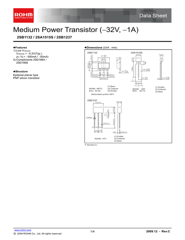
Medium Power Transistor (32V,1A)
2SB1132 / 2SA1515S / 2SB1237
2SB1132
2SA1515S
4+
− 0.2
1.5 +0.2
−0.1
(1)
0.4 +
− 0.1
1.5 +
− 0.1
(2)
(3)
0.4 +0.1
−0.05
0.5 +
− 0.1
0.4 0.1
1.5 +
− 0.1
3.0 +
− 0.2
5
Abbreviated symbol: BA
(2)
14.5 +
− 0.5
(3)
2.54 2.54
1.05
ROHM : ATV
∗ Denotes h
1/4
(1) Emitter
(2) Collector
(3) Base
4.4 +
− 0.2
0.9
0.5 +
− 0.1
www.rohm.com
0.45 +0.15
−0.05
1.0
0.65Max.
c 2009 ROHM Co., Ltd. All rights reserved.
○
0.5
2.5 +
− 0.2
6.8 +
− 0.2
(1)
2.5 +0.4
−0.1
ROHM : SPT
EIAJ : SC-72
∗
2SB1237
0.45 +0.15
−0.05
(1) (2) (3)
(1) Base
(2) Collector
(3) Emitter
ROHM : MPT3
EIAJ : SC-62
2+
− 0.2
3Min.
4.0 +
− 0.3
2.5 +0.2
−0.1
1.6 +
− 0.1
3+
− 0.2
0.5 +
− 0.1
4.5 +0.2
−0.1
(15Min.)
Structure
Epitaxial planar type
PNP silicon transistor
Dimensions (Unit : mm)
1.0 +
− 0.2
Features
1) Low VCE(sat).
VCE(sat) = 0.2V(Typ.)
(IC / IB = 500mA / 50mA)
2) Compliments 2SD1664 /
2SD1858
0.45 +
− 0.1
(1) Emitter
(2) Collector
(3) Base
FE
2009.12 - Rev.C
2SB1132 / 2SA1515S / 2SB1237
Data Sheet
Absolute maximum ratings (Ta=25C)
Symbol
Parameter
Limits
Unit
Collector-base voltage
VCBO
−40
V
Collector-emitter voltage
VCEO
−32
V
Emitter-base voltage
VEBO
−5
V
IC
Collector current
−1
A(DC)
−2
A(Pulse)
∗1
W
∗2
0.5
2SB1132
2
Collector power
dissipation
2SA1515S
PC
0.3
∗3
1
2SB1237
Junction temperature
Tj
150
C
Storage temperature
Tstg
−55 to +150
C
+
Single pulse, Pw=100ms
When mounted on a 40 40 0.7 mm ceramic board.
Printed circuit board, 1.7 mm thick, collector copper plating 100mm2 or larger.
+
∗1
∗2
∗3
Electrical characteristics (Ta=25C)
Symbol
Min.
Typ.
Max.
Collector-base breakdown voltage
BVCBO
−40
−
−
V
IC= −50μA
Collector-emitter breakdown voltage
BVCEO
−32
−
−
V
IC= −1mA
Emitter-base breakdown voltage
BVEBO
−5
−
−
V
IE= −50μA
ICBO
−
−
−0.5
μA
VCB= −20V
IEBO
−
−
−0.5
μA
VEB= −4V
VCE(sat)
−
−0.2
−0.5
V
IC/IB= −500mA/−50mA
120
−
390
−
120
−
390
−
Parameter
Collector cutoff current
Emitter cutoff current
Collector-emitter saturation voltage
2SB1132, 2SB1237
DC current
transfer ratio
2SA1515S
hFE
Unit
Transition frequency
fT
−
150
−
MHz
Output capacitance
Cob
−
20
30
pF
Conditions
VCE= −3V, IC= −0.1A
∗
∗
VCE= −5V, IE=50mA, f=30MHz
VCB= −10V, IE=0A, f=1MHz
∗ Measured using pulse current.
Packaging specifications and hFE
Package
Taping
Code
T100
TP
TU2
Basic ordering unit (pieces)
1000
5000
2500
−
−
Type
hFE
2SB1132
QR
2SA1515S
QR
−
2SB1237
QR
−
−
−
hFE values are classified as follows :
Item
Q
R
hFE
120 to 270
180 to 390
www.rohm.com
c 2009 ROHM Co., Ltd. All rights reserved.
○
2/4
2009.12 - Rev.C
2SB1132 / 2SA1515S / 2SB1237
Data Sheet
Electrical characteristics curves
-50
Ta=100 C
25 C
−55 C
-20
-10
-5
1000
−2.0
−1.5
−300
−1.0
−200
−0.5
−100
0
0
-0.2 -0.4 -0.6 -0.8 -1.0 -1.2 -1.4 -1.6
−0.4
−0.8
−1.2
500
VCE= −3V
−1V
200
100
50
IB=0mA
−1.6
−2.0
−1
−2
−5 −10 −20
−50 −100 −200 −500 −1000
Fig.1 Grounded emitter
propagation characteristics
Fig.2 Grounded emitter output
characteristics
Fig.3 DC current gain vs.
collector current(Ι)
1000
500
Ta=100 C
25 C
200
−55 C
100
50
−2
−5 −10 −20
−50 −100 −200 −500−1000
−0.2
−0.1
−0.05
−0.02
−0.01
−1 −2
−5 −10 −20
−50 −100 −200 −500 −1000 −2000
−1.0
Ta=25 C
−0.8
−0.6
lC= −500mA
−0.4
−0.2
lC= −300mA
0
−1
−2
−5
−10
−20
−50 −100
COLLECTOR CURRENT : IC (mA)
COLLECTOR CURRENT : IC (mA)
BASE CURRENT : IB (mA)
Fig.4 DC current gain vs.
collector current(ΙΙ)
Fig.5 Collector-emitter saturation
voltage vs. collector current
Fig.6 Collector-emitter saturation
voltage vs. base current
Ta=25 C
VCE= −5V
−2
−5
−10
−20
−50 −100
EMITTER CURRENT : IE (mA)
Fig.7 Gain bandwidth product
vs. emitter current
www.rohm.com
c 2009 ROHM Co., Ltd. All rights reserved.
○
50
20
10
−0.5
−1
−2
−5
−10
−20
COLLECTOR TO BASE VOLTAGE : VCB (V)
Fig.8 Collector output capacitance
vs.collector-base voltage
3/4
−2
−1
−0.5
∗
50
Ta=25 C
f=1MHz
IE=0A
s
0m
=1 ∗
P w ms
00
100
−5
100
=1
Pw
200
20
−1
−0.5
Ta=25 C
IC/IB=10
COLLECTOR CURRENT : IC (A)
−1
−1
COLLECTOR TO EMITTER VOLTAGE : VCE (V)
COLLECTOR CURRENT : IC (mA)
COLLECTOR SATURATION VOLTAGE : VCE(sat )(V)
BASE TO EMITTER VOLTAGE : VBE (V)
COLLECTOR TO EMITTER VOLTAGE : VCE (V)
VCE= −3V
DC CURRENT GAIN : hFE
Ta=25 C
Ta=25 C
−2.5
-2
-1
0
TRANSITION FREQUENCY : fT (MHz)
−3.0
−3.5
−4.0
−400 −4.5
−5.0
DC CURRENT GAIN : hFE
-200
-100
−500
COLLECTOR CURRENT : IC (mA)
VCE= −6V
COLLECTOR OUTPUT CAPACITANCE : Cob (pF)
COLLECTOR CURRENT : IC (mA)
-500
D
−0.2
C
−0.1
−0.05
−0.02 Ta=25 C
∗Single pulse
−0.01
0 −0.2 −0.5 −1
−2
−5 −10 −20
−50
COLLECTOR TO EMITTER VOLTAGE : VCE (V)
Fig.9 Safe operation area
(2SB1132)
2009.12 - Rev.C
100
10
1
0.1
0.001
−5
Ta=25 C
0.01
0.1
1
10
100
1000
TIME : t (s)
Fig.10 Transient thermal resistance
(2SB1132)
www.rohm.com
c 2009 ROHM Co., Ltd. All rights reserved.
○
−2
200
Ta=25 C
∗Single pulse
IC Max.∗
−1
−0.5
PW =10ms∗
∗
−0.2
Ta=25 C
100
TRANSIENT THERMAL
RESISTANCE : Rth ( C/W)
1000
Data Sheet
COLLECTOR CURRENT : IC (A)
TRANSIENT THERMAL RESISTANCE : Rth ( C/W)
2SB1132 / 2SA1515S / 2SB1237
PW =100ms
DC
−0.1
−0.05
50
20
10
5
−0.02
−0.01
−0.1 −0.2
−0.5 −1
−2
−5 −10 −20
−50
COLLECTOR TO EMITTER VOLTAGE : VCE (V)
Fig.11 Safe operation area
(2SB1237)
4/4
2
0.01
0.1
1
10
100
1000
TIME : t (s)
Fig.12 Transient thermal resistance
(2SB1237)
2009.12 - Rev.C
Notice
Notes
1) The information contained herein is subject to change without notice.
2) Before you use our Products, please contact our sales representative and verify the latest specifications :
3) Although ROHM is continuously working to improve product reliability and quality, semiconductors can break down and malfunction due to various factors.
Therefore, in order to prevent personal injury or fire arising from failure, please take safety
measures such as complying with the derating characteristics, implementing redundant and
fire prevention designs, and utilizing backups and fail-safe procedures. ROHM shall have no
responsibility for any damages arising out of the use of our Poducts beyond the rating specified by
ROHM.
4) Examples of application circuits, circuit constants and any other information contained herein are
provided only to illustrate the standard usage and operations of the Products. The peripheral
conditions must be taken into account when designing circuits for mass production.
5) The technical information specified herein is intended only to show the typical functions of and
examples of application circuits for the Products. ROHM does not grant you, explicitly or implicitly,
any license to use or exercise intellectual property or other rights held by ROHM or any other
parties. ROHM shall have no responsibility whatsoever for any dispute arising out of the use of
such technical information.
6) The Products are intended for use in general electronic equipment (i.e. AV/OA devices, communication, consumer systems, gaming/entertainment sets) as well as the applications indicated in
this document.
7) The Products specified in this document are not designed to be radiation tolerant.
8) For use of our Products in applications requiring a high degree of reliability (as exemplified
below), please contact and consult with a ROHM representative : transportation equipment (i.e.
cars, ships, trains), primary communication equipment, traffic lights, fire/crime prevention, safety
equipment, medical systems, servers, solar cells, and power transmission systems.
9) Do not use our Products in applications requiring extremely high reliability, such as aerospace
equipment, nuclear power control systems, and submarine repeaters.
10) ROHM shall have no responsibility for any damages or injury arising from non-compliance with
the recommended usage conditions and specifications contained herein.
11) ROHM has used reasonable care to ensur the accuracy of the information contained in this
document. However, ROHM does not warrants that such information is error-free, and ROHM
shall have no responsibility for any damages arising from any inaccuracy or misprint of such
information.
12) Please use the Products in accordance with any applicable environmental laws and regulations,
such as the RoHS Directive. For more details, including RoHS compatibility, please contact a
ROHM sales office. ROHM shall have no responsibility for any damages or losses resulting
non-compliance with any applicable laws or regulations.
13) When providing our Products and technologies contained in this document to other countries,
you must abide by the procedures and provisions stipulated in all applicable export laws and
regulations, including without limitation the US Export Administration Regulations and the Foreign
Exchange and Foreign Trade Act.
14) This document, in part or in whole, may not be reprinted or reproduced without prior consent of
ROHM.
Thank you for your accessing to ROHM product informations.
More detail product informations and catalogs are available, please contact us.
ROHM Customer Support System
http://www.rohm.com/contact/
www.rohm.com
© 2013 ROHM Co., Ltd. All rights reserved.
R1102A
