Precision etching of micro components
advertisement
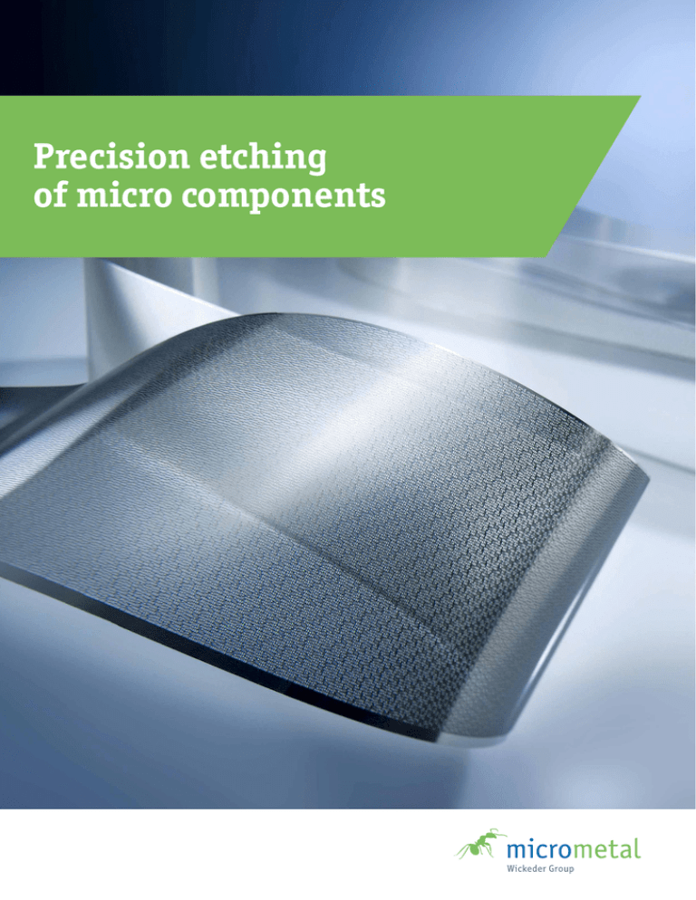
Precision etching of micro components A High-Tech Profile Micrometal manufactures customized, highly accurate etched components. We photochemically etch these parts from thin materials (starting at 0.025 mm) in extremely high quantities. Unique: Our Inline etching facility enables highest precision at high reproducibility and cost efficiency, amongst others, by use of wet lacquer and high-precision glass tools. Micrometal stands for microsystem technology know-how accumulated over decades. Our production facilities are located at the border triangle Germany France - Switzerland. The chemical precision etching process is certified to ISO TS 16949 and DIN EN ISO 14001. High precision etching... ...infinitely! Photochemical etching - uniquely precise Micrometal is at home in the world of ultra-tight tolerances, fine structures, thin metals, and complex shapes. Applying a special Inline production technology Micrometal can etch sheets ranging from 0.025 to 0.500 mm thickness. Advantages The metal etching technology developed by Micrometal significantly differs from conventional techniques. The customer´s data are processed via CAD to create an individual glass tool. The material chosen by the customer - available as coil - is cleaned and then coated with photoresist on both sides. Usually a relatively thick dry film resist is applied but Micrometal uses a special wet lacquer system to obtain ultra-thin photoresist layers resulting in a higher grade of precision. In a UV lithography process the metal strip is exposed with the glass tool. After the developer the selectively coated metal strip undergoes photochemical etching. During this process the sheet can be structured with a great variety of different geometries. After cleaning and drying full automatic inspection is performed. As per individual customer request the finished metal strip is supplied on reels, as sheets or as single parts. A continuous single strip can have a length of up to 800 m. › Stress- and burr-free › Unique precision › A variety of metals and alloys: › Stainless steels and other steel alloys › Nickel and cobalt base materials › Copper and copper alloys › Amorphous/nanocrystalline materials › Industrial use and special applications › Ready-to-ship products on reels, or as sheets or as single parts for direct further finishing on your production line › Customized total solutions featuring additional value, by collaboration with our industrial partners Finest structures – tightest tolerances We set the standards in our industry Automotive Medical Devices Chemical Industry Consumer & Capital Goods The Inline lithography etching process is an excellent tool for the manufacturing of highly-precise metal parts in industrial quantities. Even the most complex components can be realized respecting the tightest tolerances according to your specifications. Filters & sieves Especially for applications requiring a large number of holes with identical or different geometries the Micrometal etching technology offers a significant advantage: free structuring possibilities. Grid arrays and break-through geometries can be designed individually applying a damage-free production process. Thus the functionality of a sieve can be adapted to nearly all lay-outs of an application. Etched sieves are characterized by a high selectivity and very good back-flush properties. They are completely burr-free and also suitable for residue-free cleaning and subsequent sterilization. Pressure stability is another advantage especially valued by the automotive industry for applications like, e.g. filters for injection systems or protective filters for hydraulic assemblies. Possible applications for the food industry are sieves for coffee machines and sugar production. Needles & blades The Micrometal etching technique meets the extremely tight specifications of medical technology and here our standards are industry-leading. Due to variable design parameters break-through geometries can be realized using special 3D shapes. This enables largescale production of complex geometries for lancets, scalpels, and blades. Additional advantages: no stress is induced material and the chemical as well as the properties remain unchanged. These are arguments for applying this technology production of micro-surgical instruments, combs for medical use. into the physical decisive in the saws or Surface & function Special process parameters applied in mask preparation and the exposure systems allow the structuring of different, highly-precise geometries on both sides of the same component. Thus a large variety of surface effects can be realized, e.g. defined half etch areas and the production of combination structures. These properties find their application in the production of micro-fluid products, optical surface effects as well as tribological functional surfaces. Precision & more Customers across the industries already value our Inline lithography etching technology as an alternative to conventional techniques. In cooperation with our partners we can offer you further processing like injection molding, forming, diffusion welding, laser welding or selective coating. We supply microprecision components worldwide and we are looking forward to accepting new challenges – especially from industries we do not yet serve. Photo etching technique in all its variety Micrometal is capable of processing metal of thicknesses ranging from 0.025 to 0.500 mm and a source material width of up to 315 mm. A minimum hole diameter of 80 % of the material thickness can be realized. Coil thickness Smallest hole diameter Diameter tolerance 0.025 0.02 +/- 0.0050- 0.050 0.04 +/- 0.007 0.100 0.08 +/- 0.010 0.150 0.12 +/- 0.012 0.300 0.24 +/- 0.035 0.500 0.40 +/- 0.050 Best of metal. The metal specialists of Wickeder Group combine their expertise to offer you the best of metal. On three continents (Europe, North America, and Asia), there is a wide range of standard and customized solutions. We can guarantee highest quality standards, flexibility, and fast response times by our product- and service- oriented business model. Ultramodern production lines, extensive knowledge, and innovative solutions have always been the success of Wickeder Group. Achievable hole geometries Engineered Materials Solutions Deutsche Nickel Wickeder Westfalenstahl Engineered Materials Solutions Auerhammer Metallwerk Micrometal Engineered Engineered Materials Materials Solutions Solutions Dimensions in mm For more detailed information please visit www.micrometal.de Deutsche Nickel Portfolio of Micrometal Portfolio of Wickeder Group : › Filters › Implantate › Leadframes › Sieves › Kodierscheiben › Grids › Technische Federn › Pins › Funktionsoberflächen › Contacts › Diffusers › Comprehensive, single-supplier solutions › Clad Materials › Thermostatic Bimetals › Metal Strips & Metallic Foils › Bars & Wires › Precision-etched Micro Components www.wickeder-group.com www.micrometal.de micrometal GmbH Renkenrunsstrasse 24 79379 Muellheim (Baden), Germany Phone +49 7631 936 88-0 info@micrometal.de
