MOSFETs in comparison with BJTs
advertisement
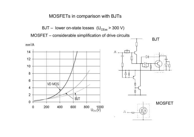
MOSFETs in comparison with BJTs BJT – lower on-state losses (UCEss > 300 V) MOSFET – considerable simplification of drive circuits BJT MOSFET VD MOS IGBT IGBT (Insulating Gate Bipolar Tranzistor) Although the IGBT structure may appear very similar to that of the VDMOS transistor, its function is rather different As with a MOSFET, the application to the gate of a positive voltage, VGE> VGE(th), creates a conducting channel between the N+ and N regions. This forward biases junction, J1, and holes are injected from the p+-emitter of the P+NP transistor into the N-base. The hole current which crosses junction J2 (the collector current of the PNP transistor) α pnp I n I p = 1α pnp where In is the electron current passing through the channel of the MOS transistor If gate-emitter voltage VGE > VGE(th) is high enough In = As far as IE = Ip + In, IE = IC = In z µeff Cox (VGE − VGE(th) )Vch l 1- α pnp the collector current of the IGBT can be expressed as IC = z µeff Cox (VGE − VGE(th) )Vch l (1 − α pnp ) When the channel voltage exceeds (VGE - VGE(th)), the collector current saturates IC = 1 z µ eff Cox (VGE − VGE(th) )2 2α l (1 − α pnp ) The transconductance of the IGBT g fs = The transconductance of the IGBT in saturation is g fs = ∂ IC ∂ VGE VCE =const µeff Cox (VGE − VGE(th) ) α l (1 − α pnp ) z The on-state characteristics of the IGBT The main conduction path through an IGBT can be modelled as a diode in series with an MOS transistor. The diode current IF = (1 - αPNP)IC E C G JF = The current density JF flowing through the diode area Sd Forward voltage drop VF across the diode VF = K 0 + K1 ln J F + K 2 J F Vch = The voltage drop across the MOS channel µeff ox GE Sd m (1 − α )I l C z (V − V pnp 1 C GE(th) (1 − α PNP )I C VF = VT 0 + rT I F ) VCE(on) (I C ) = Vch (IC ) + VF (I C ) The total on-state voltage drop Using a linear approximation of the I-V characteristic VCE ( on ) = VTO + (1 − α ) l C z (V − V pnp µeff ox GE GE(th) ) I C + rT (1 − α pnp )I C = VTO + rT* I C The maximum blocking voltage is limited by the breakdown voltage, VCEO, of the PNP+ transistor. Two basic construction are used: NPT IGBT The problem is similar to the one described in detail for thyristors, i.e., the base thickness and donor concentration in the base have to be optimised PT IGBT A compressed field structure obtained by forming an N+ layer of about 10 µm thickness between the P+ collector layer and the N-base is often used to combine a high blocking voltage with a low on-state voltage IGBT Switching Characteristics The beginning of the IGBT turn-on process is closely related to the turn-on process of a power MOSFET td(on) = VGE + RG (CGE + CGC )ln 2 Dp VGE − VGE(th) 2 wpnp IGBTs have a current handling capacity that is approximately an order of magnitude higher than that of an equivalent VDMOS transistor. Therefore, the area of silicon wafer necessary for an IGBT with the same nominal current is a similar magnitude lower. However, this means that CGE and CGC are lower in the same ratio for devices having the same nominal current rating.. Simultaneous solution of equations, taking account of the variation of the capacitance, CGE, and the current gain of the bipolar transistor, is very complicated. Numerical solution is required. IGBT Turn-off Process Part of the total on-state electron current that passes through the MOS channel is controlled by the gate charge. For this to be interrupted, the gate capacitance has to be discharged As soon as VGE decreases below VGE(th), the MOS channel is turned-off. ( ) ∆I C = I n = 1 − α pnp I C The collector-emitter voltage then rises so that its rate of rise is given by dVCE g fsVGE(th) + IC = dt g fs RG CGC Tail current −t τ eff I C ( t ) = α pnp I C ( 0) exp Turn-off losses Woff ≈ VC0 ICα pnpτ eff Trench IGBT IGBT RC IGBT RB IGBT Different vertical IGBT designs a) PT IGBT b) NPT IGBT c) SPT IGBT
